Enrico
-
Forgottings: forgotthings
06/01/2017 at 22:25 • 0 commentsI have realized only now that the VHDL code was not available from GitHub. Now it is back, and can be accessed from the links (in the ice40 folder).
And no, no improvements. Too many other new ideas, too little time, for now.
-
[Test] A brief demo of the buttons and the serial commands
01/04/2017 at 23:09 • 0 commentsHere is attached the link of the videos which are showing the utilization of the system.
The first video is a raw button interaction, where I try to select one mode and check what it is by pushing the up and down buttons. If changes the intensity in a discrete way, it is the intensity mode, otherwise it changes the white saturation or selects the color. The button is acquired from the Atmega, which selects, according to the mode, the intensity, white or color and send it in to the FPGA fabric. From there, the PWM output is connected to the 4 LED drivers powered from 9V wall adapter.
The second video is the serial data interpretation. The tool used is a Python one in the links of the project. The tested color pattern is the following, where it is represented in #RRGGBB:
#000000 (all is off), #39ec20, #ff0d0d, #16b8f5, #eb1cf0, #f8ad14, #fef9ed, #403d31, #000000 (all is off).
The data is packed according to a protocol described in the logs, sent to the Atmega and then transferred to the FPGA logic.
Remember that the switch between the serial mode and the user buttons mode is made just by pressing any button or by sending a complete frame over serial. The last mode will take over the previous one, but all the data of the last mode is kept in the Atmega's memory so that when the user will press a button, the previous setting is restored.
-
[FW] The butchered code
01/04/2017 at 22:12 • 0 commentsThe initial, ideal version of the firmware was used on other projects, like this. It was implementing every step of the color generation, from the autowhite adjustment, to the main color selection, the PWM generation, the power monitor, the serial commands, the encoder management and so on. Everything in 8098 kB of program memory, and 368 bytes of RAM.
Cutting out almost 90% of the code was an overwhelming challenge. The main constraint was my idea to stick with the RGB project for the 1kB Challenge, instead focusing on something else. And for pure coincidence I had also bought a Lattice FPGA. Then the works has just started: what could be moved away from the software and that can be represented in raw logic? How can the information be passed between the microcontroller and the FPGA?
The result is an hated spaghetti code, with no safety features from the ADC for the power monitoring, no encoder management and so on. The only thing was to rely as much as possible on the MCU hardware, for the UART, PWM and.... no, there are no pins available and there is no way to implement any protocol in bit banged way.
And now I realized that the only thing that keep a soul in the MCU is the data management from the user and the overall control. Moreover, also the data management from UART is kept inside the MCU, since it was implementing all the characters filtering and the numeric conversions. In this way, the user can still manage the double functionality, which is from hexadecimal commands from serial or using 3 buttons (instead of a rotary encoder).
All the functions were optimized accordingto the ASCII tables that allow huge data compression. A snippet of the original character conversion function:
static unsigned char lamp_c2h(unsigned char msb, unsigned char lsb){
	if ((msb < 'a' && msb > '9') || msb < '0' || msb > 'f' ||
	(lsb < 'a' && lsb > '9') || lsb < '0' || lsb > 'f'){
		// printf("Not HEX value. msb: %c, lsb: %c\n", msb, lsb);
		return 0;
	}
	if (msb >= 'a' && msb <= 'f'){
		msb = msb - 'a' + 10;
		} else {
		msb = msb - '0';
	}
	if (lsb >= 'a' && lsb <= 'f'){
		lsb = lsb - 'a' + 10;
		} else {
		lsb = lsb - '0';
	}
	return (lsb+(msb*16));
}
became this:
static unsigned char lamp_c2h(unsigned char msb){
    uint8_t tmp = 0;
    tmp = msb;
    msb=msb&0x0F ;
    if (tmp>'9')
    msb+=9;
    return (msb);
}
And I also learned how a shift instruction could take a lot of space, when you start noticing every single byte eaten up by your code.The double edge weapon of the hardware relief
In this way a small SPI master control is written, in order to send the correct data to the FPGA. Again, you can feel how much work you move away from the MCU's processor (and so from the memory occupation) when you have a dedicated HW that does the job.
And I am not talking about the FPGA, but I am referring on how just the SPI hardware of the Atmega was of huge help in memory reduction, try to think in implement this in firmware, how much more space have been taken off? This is obvious, but not always appreciated.
A byte assignment in the FW, and a lot of stuff moving in the hardware. That is fun...or, no, not when you have to deal with designing another piece of hardware that shall receive all that beauty from the SPI of the Atmega. And now I am talking about the FPGA.
The final memory status
Or the final countdown to 1024 bytes. At the end, I discovered that I was trained to freeing up the RAM. To me, was way more tricky to find out how to save on byte from flash rather than from RAM.
This meas that for coincidence I have freed the 92% of the RAM. While my efforts were in freeing up the program memory, which now is reduced by the 88%.
As a result, this is my memory implementation, from the build output of the Atmel Studio 7:
Program Memory Usage : 954 bytes 2,9 % Full
Data Memory Usage : 29 bytes 1,4 % Full -
[HDL] The FPGA design
01/04/2017 at 21:33 • 0 commentsTop level description
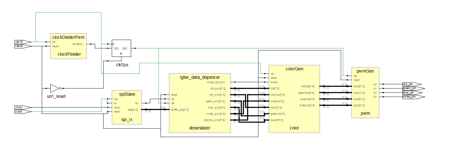
Here is shown the top-level implementation, written in VHDL and synthesized using free licence tools from Lattice, which are the Diamond LSE for the sysnthesys, Diamond Programmer Tool for flashing the configuration memory, ICE Cube for the P&R and the integration of the LSE tool, Aldec Active HDL for the simulation.
![]()
In the top level, you can spot the SPI slave, which sends data to the Deserializer, where on its turn splits the data in paraller and synchronous way to the Color Generator. This module will implement the intensity management, the white saturation, the color and the mode. The mode simply instruct the Color Generator to excludes all the white, intensity and color management and follow the SPI data. Otherwise, will ignore the RGBW data from the SPI and generates it according to an index, generated in the Atmega.
The original idea was to send back the data to the MCU, but then I realized that I have not enough pins, so in the FPGA it is also implemented a 4 channel PWM module.
Nice similarities in Atmega products
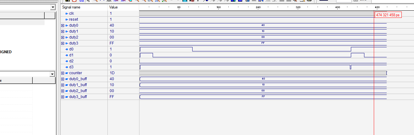
It is nice to see that my PWM have the same bug as the Atmega: it cannot swing from 0 to 100%, but it will have a glitch. So the minimum is 1/255 if not inverted or the maximum can be 254/255 if inverted. I simply inverted internally the control circuitry, so that I have a PWM that swing from 0/255 up to 254/255, but it is a not inverted type. In this way, this glitch cannot be seen. This glitch is totally normal in a raw implementation, and can be easily masked. I wonder why it isn't in Atmegas. What a lazy one the designer.
Below a simulation snapshot showing the glitch on D3 signal:
![]()
Overall FPGA utilization
The FPGA itself is almost full, especially when optimizing for speed. This project gives to me some feedback on how really problematic could be an HDL design when you have few resources. For example, I have initially implemented a division, a combinatorial default one: 50% of the FPGA was filled with this logic, while the other 50% shall be filled with 80% of resources. My iCE40 does not have the 130% of space.
So the division for implmenting the dimming was made by issuing a dynamic shift in the Color Generator, reducing the dimming steps for the user. In the Atmega, a division was performed very well. But the previous code was fine tuned, smooth and big 8kB more.
-
[HW] The overall schematics
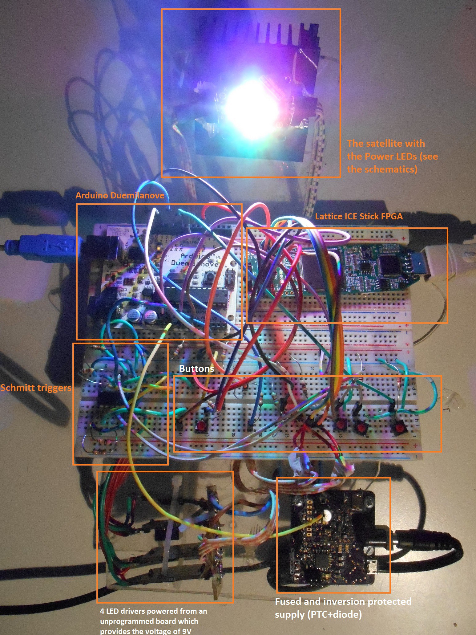
01/02/2017 at 22:41 • 0 commentsSince this project is all breadboarded, I will share the schematics (and pictures) since there is no a real layout, and Fritzing would became insanely complex. Below, a picture with the regions herein described through the schematics and the connections, just to make the wirings not too overwhelming:
![]()
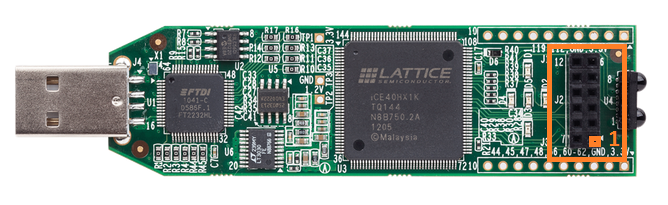
Here you can see the iCE Stick FPGA used, and the highlighted in orange connector J2, and pin 1 highlighted too:
![]()
From here, I am referring to the FPGA connections as iCE Stick header J2 pin XX.
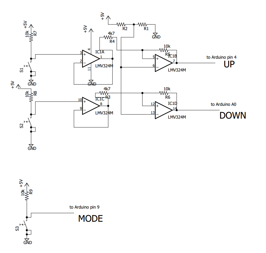
The hardware debounce for the UP and DOWN is made using a schmitt trigger obtained through an LM324, while the MODE is simply a pull-up which works nice in the firmware which somehow filters away some glithes (a cap shall be added, btw):![]()
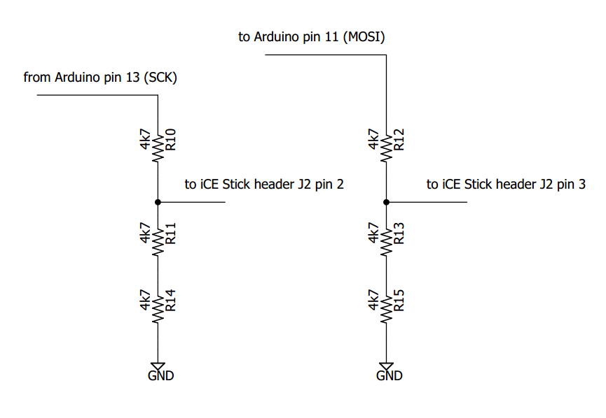
The communication between the Arduino and the FPGA happens through unilateral SPI communication, so that a simple 2/3 resistor voltage divider is sufficient to safely connecting the 3.3V FPGA to the 5V Atmega:
![]()
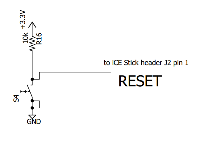
If needed, it is provided a RESET buttons to re-initialize the FPGA:
![]()
If you take the entire VHDL implementation "as is", for debugging purposes you will see the SCK pin redirected on ICE board LED D1, while the other 4 color signals are also duplicated on the remaining ICE debugging LEDs.
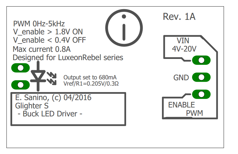
The output of the FPGA is feeding the power LEDs through a module that I've build few months ago, but you can power up anything else. Here you can see a picture of one module which can be fed with a PWM signal as high as the supply voltage, where such supply can be as high as 20V. As already said, you can connect any LED to try out the Arduino+FPGA setup.
Here is the module, powered at 9V, where the PWM swings between GND and 3.3V of the ICE Stick:
![Power LED module]()
The LED connections is shown on the board too.
Here you can see the briefing of the entire connection setup within this log, where some of them are conditioned using the above schematics (all names are referred as in the schematics, so that you can reproduce the connections):
- RESET active low button S4 -> FPGA J2 pin 1
- Arduino pin 13 -> FPGA J2 pin 2
- Arduino pin 11 -> FPGA J2 pin 3
- One active low switch S1 -> Arduino pin 4
- One active low switch S2 -> Arduino pin Analog 0
- FPGA J2 pin 7 -> enable/PWM pin RED driver
- FPGA J2 pin 8 -> enable/PWM pin GREEN driver
- FPGA J2 pin 9 -> enable/PWM pin BLUE driver
- FPGA J2 pin 10 -> enable/PWM pin WHITE driver
Remember to keep the GND reference between Arduino, ICE Stick and all the 4 LED drivers in order to avoid fire. The 4 LED drivers are soldered on perfboard and a 4 wire strips is connected in J2 of the ICE Stick.
You can spot a second board, which provides power to the LEDs: it mounts a second Atmega which is not used. That board (a Lino board) was lying around and I decided to use it, since I am also late in the submission for the challenge. It provides only few basic electrical protections. :)
Hardware based RGBW Lamp controller
Or how to write firmware the weird way to submit a project in the 1kB Challenge.