This tutorial was done on Windows. Authors claim it could also be used on Linux by using Mono, but I haven't tried and don't understand a lot about Mono to see what could be done. I am switching to Linux nowadays, so I'd be very grateful to anybody that'd make instructions on how to launch it, however - and I'm sure other fellow Linux-wielding engineers will be grateful, too =)
This is the GitHub issue describing steps to launch it on Linux, half-successfully (thanks to @jlbrian7 for figuring this out)
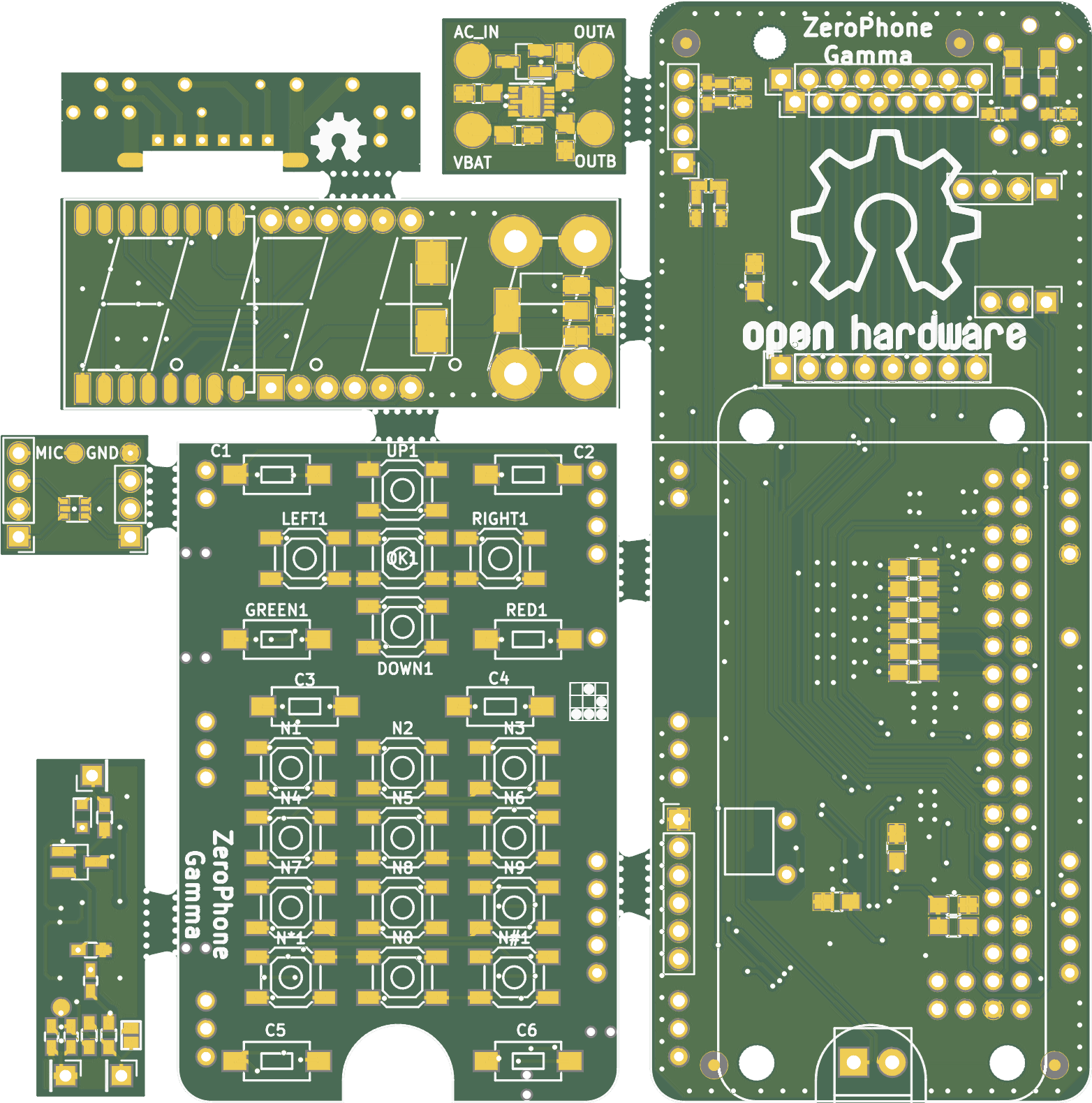
The tool I'm personally using to panelize boards is GerberPanelizer from ThisIsNotRocketScience.nl. It's a wonderful tool that allows you to panelize PCBs, mainly using tabs&mousebites. There are more tools in the archive, they all seem Gerber-related but I didn't even go through them =)
I'm using KiCad myself, so I'll mainly work with KiCad-made gerbers. The panelizer project page has some tips for Eagle users as well, related to CAM files, so if you're an Eagle user, check it out, it can help with some moments. I'd love to cover Gerber generation for different EDA packages (actually, not), but Internet has plenty of tutorials on those. There's a good online Gerber files viewer (needs gerber ZIPs) which gives out pretty renderings of your board, so you can use it to check your Gerbers - I do that all the time (and KiCad 3D viewer helps, too).
No matter your EDA tool, the workflow is simple - first, you have to have gerber files in separate folders for each project.
Gerber export tutorial - KiCad (with important Panelizer-specific notes)
Generate gerbers for each project that you want to include on the panel. You should have a couple of separate folders with gerber files - or in case you want to panelize multiples of the same board, just one folder.
Gerber folder requirements:
- Just a folder, named however you like, with Gerber files inside (not zipped up or anything)
- Only one board per folder allowed
- Files can be in ".gbr" format (where extension is the same but filenames differ), judging from the code, but I haven't checked if it works.
- Otherwise, has to have a .gml/.gko file - .gm1 from KiCad isn't suitable yet (but will hopefully be at some point)
The workflow is simple - drag a folder from your file manager onto the view, and the board inside the folder will be added.
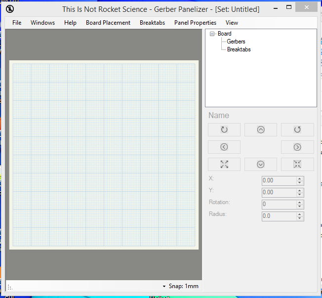
To start, open the GerberPanelizer tool. Go to File->New:

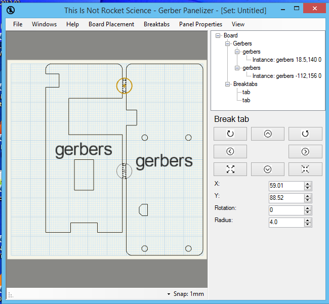
Now, you need to drag a folder with gerbers onto the view. The collapsible list in the right top corner will indicate there's a board and, if you're lucky, it's going to appear on the field, too.
Necessary: leave some distance between adjacent boards: the mill bit that will be milling out the board outline has to have some place to move. Good distance is 2mm and up.
After we placed some boards, we need to place tabs connecting them, and I think it makes sense to do it manually. Hover mouse cursor on the space between the board and press T on keyboard, you're going to get a circle. Move that circle to the place where you want a tab and it'll link two boards. If it won't be able to, the circle outline will be red and it'll give a warning in small text, hopefully.

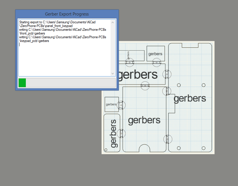
Too many tabs will make dividing boards hard. Not enough tabs will give a chance of boards breaking off and getting lost after milling. I more or less have one tab per each board in total, there's also "1 tab per 3cm" rule of thumb. This is OK:

Now, once you've rotated, moved and linked all the boards, press the File -> Export Merged Gerbers button, and make a new folder somewhere to store the gerber files in:


 Arya
Arya
Discussions
Become a Hackaday.io Member
Create an account to leave a comment. Already have an account? Log In.
Just tried this. Wow, that panelizer is painful to use, slow and waits for you to get done entering all your data before it crashes. Has no documentation to speak of, and what else?
The ThisIsNotRocketScience GerberTools is not completely worthless, however.; it serves as an example of how not to release software.
Are you sure? yes | no
Sadly the latest release from 2018 doesn't work under Linux for me, only the one named Panelizer posted by somebody in a thread you referenced works.
I also found quirks in the software. For example if position two instances of the same design head to toe by rotating one 180° and then run the packer the rotation (any angle actually) gets cancelled.
Never mind, the tool will only be used once in a while.
C# looks as horrible a language as Java. 😉
Are you sure? yes | no
wow nice new tool! i've been using gerbmerge for some time! it's much more cryptic than this tool! https://github.com/prpplague/gerbmerge
Are you sure? yes | no
This writeup will have its second birthday in a couple of days! ;-P it's probably just that you only saw this now due to the new comments. Do check out this tool, I am very happy with it - I even have a Python script to auto-combine the .pos files! https://github.com/CRImier/Panelizer2PnP
Are you sure? yes | no
Thanks, seems to work well under Linux. I used a precompiled version labelled Panelizer.zip in that github thread you referenced. Didn't check if anybody packaged a more recent version, just playing around with it before using it in earnest.
I ran it under Linux by going to the directory and
mono GerberPanelizer.exe
then driving the GUI. Naturally mono needs to be installed. I installed the package mono-core and its dependencies on my distro. .gbr format doesn't work but Protel does if you rename .gm1 to .gml. A pity as .gbr extensions are the better standard.
A little experimentation shows that mono needs to be run in the directory with the .exe and other resources so I made a little helper shell script like this:
#!/bin/sh
cd [directory with GerberPanelizer.exe]
exec mono GerberPanelizer.exe
Are you sure? yes | no
Very happy to hear that! One small comment from you, one giant leap for me gradually moving from Windows to Linux =)
Are you sure? yes | no
I take back the comment about .gbr format working. Seems only the Protel extensions work.
Are you sure? yes | no
Got it! I don't think that's Linux-specific, maybe the panelizer just doesn't understand the KiCad format? I would suggest you open an issue on GitHub, of course, look it up there too, maybe someone already figured that one out.
Are you sure? yes | no
(I personally never use the .gbr extensions, so I have no idea if they actually work on Windows)
Are you sure? yes | no
It's not a Linux or Kicad issue. The problem is the Protel file extension convention was always that, not a standard. I can imagine someone reading a printed copy of Protel documentation wasn't sure if it was .gml or .gm1. Neither is mandated by any standard so it's a WontFix issue for Kicad. The later x2 format with metadata in comments fixed that so the only extension needed is .gbr what is specified in the standard. But Panelizer doesn't understand that format. If not already done Panelizer should regard .gml and .gm1 as equivalent.
Are you sure? yes | no
Hi Aresnijs, I'm discovering Gerber Panelizer, thank you for your tuto,
do you know how to deal with the creation of breaks between the gerber files and the 'fill empty area' area ?
I'm using Version 1.0.6257.24941 built on 17/02/2017
Are you sure? yes | no
Hi! Sorry for reaching out so late, I didn't get a notification for your reply here =( I have sent in a pull request to fix this issue on GerberPanelizer GitHub, but AFAIK the PR is not merged, and the issue is not yet fixed separately. Meanwhile, I can publish a version I compiled myself, without this problem.
Are you sure? yes | no
Is there a complied version with the fix? I see that the solution still hasn't been used
Are you sure? yes | no
Here's the file : http://files.zerophone.org/GerberTools-with-fill-fix.zip ; cc @Seamus de Cleir
Are you sure? yes | no
Thanks a million
Are you sure? yes | no
@Arsenijs The file is no longer available. I'm not sure it'll solve my problem, but my problem is that I'm checking 'fill empty area' and hitting OK and the software crashes...maybe little help??
Are you sure? yes | no
I came across this tool but didn't have a chance to play with it at the moment... Seems better than doing the mouse bites by hand :)
About the KiCad origin issue, you might want to export your Gerbers (and drill file) with the "Use auxiliary axis as origin" option. In KiCad you can place that auxiliary origin with one of the buttons in the toolbar.
Are you sure? yes | no
Added the instructions for the "auxiliary origin point" thing, hope nobody misses it when following the instructions =)
Are you sure? yes | no
I needed JUST this... thanks
Are you sure? yes | no
If this is useful to you, and you have some small boards that would be useful to others, please do share them on this project =)
Are you sure? yes | no
@Arsenijs Thanks, this looks good, I'll give it a try on my next board. One of my issues is trying to keep the order# the board house puts on off my actual boards. Have you had any experience with trying to tell them where to put it?
Are you sure? yes | no
As far as I know, DirtyPCBs, for example, doesn't care and will put it wherever. Other fabs, however, don't put them at all. I'd say it's very fab-specific, but I'm guessing that if you have part of your board full with silkscreen art and another part is empty, they'll most likely put it on the empty part.
But then, I don't know if it's not automated =D
Are you sure? yes | no
PCBWay actually states this on their website "Attention please! If you don't note not to add pcb order number on board, we will add it on board by default!"
What they do is let you enter an order (eg dimensions, quantity, color etc) without uploading a PCB file. After your order is entered, they give you an order number, e.g. "1234567". Then you can go back and modify your PCB to add the number, "1234567" somewhere on the board (probably would be a good idea to let them know where you put it as a comment). DISCLAIMER: I haven't actually tried this before.
The funny thing about how they charge - it costs extra if you put multiple DIFFERENT designs on one board. However if you put multiple copies of the SAME design on one board, they don't charge extra.
Are you sure? yes | no
BTW, I ordered two identical panels from DirtyPCBs, and the order numbers were in different places, even though the gerbers were identical =)
Are you sure? yes | no
@Arsenijs All this talk of order# made me look at a board I had made. It took some searching but I found the order number PCBway put in 1 mm lettering under one IC footprint. That size wouldn't bother me at all.
Another fab I used, elecrow, didn't put an order# at all. And they also offer V-cut and mouse bite panelizing for free for identical designs on one board but you have to give the instructions in separate notes.
Are you sure? yes | no
@leb9049 Check this tutorial out =)
Are you sure? yes | no