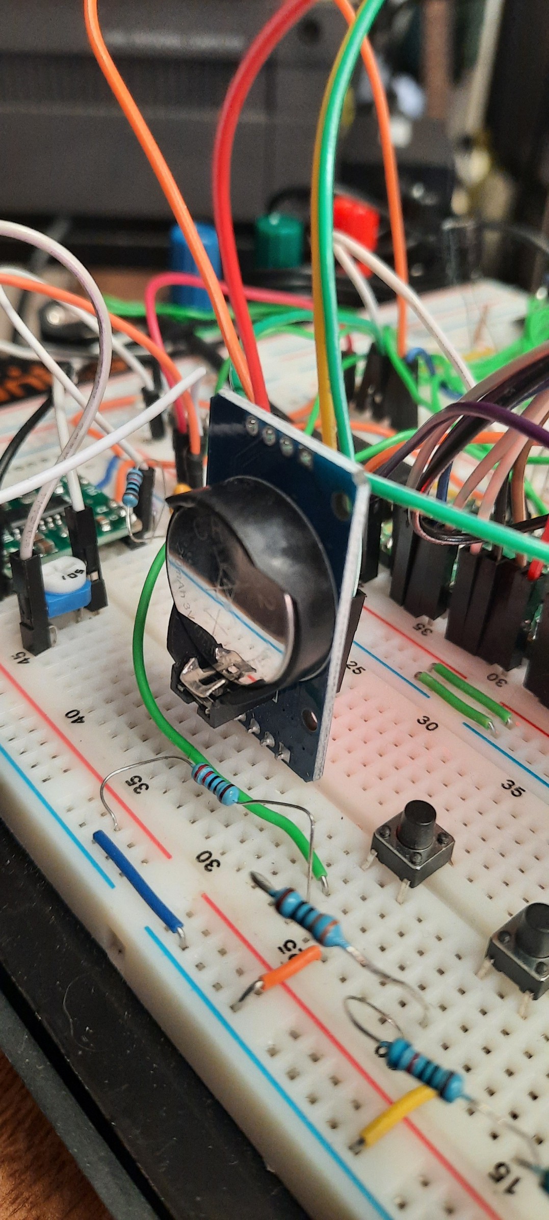
In my original RetroChallenge 2023/10 participation announcement, I promised a battery backed-up Real Time Clock (RTC) for the Microtronic. Well, here it is! I have hooked up the DS3231 RTC.
So how does that work? See, the Microtronic already has an internal real time clock in its firmware, and there is even an op-code F06 ("load time") that can be used to load the current time to register memory (registers for A-B for hours, C-D for minutes, and E-F for seconds). Two built-in ROM programs (PGM 3 and PGM 4) also allow you to set and see the current time (without using the F06 op-code).
However, the Microtronic RTC is not battery backed-up, and hence if you want to use the real time in your programs, you will always have to set the clock manually when you turn it on (using the ROM program PGM 3). This of course means limited utility.
How can the DS3231 RTC help here? Well, using similar ideas as explained in my previous log entry https://hackaday.io/project/192655-picoram-2090/log/224467-retrochallenge-202310-log-entry-3, instead of adding extra side-effects / semantics to vacuous op-codes, I can also intercept a non-vacuous op-code such as F06 ("load time"), and do anything I want by switching first into a dedicated memory bank to not interfere with the current program, then execute this program with the Microtronic, and finally return to the original program. When F06 is intercepted, the Pico first retrieves the current time from the DS3231, and then materializes a set of MOVI nx = Move Immediate Value n to Register x(op-code 1nx) into the current memory bank that will, when executed by the Microtronic, write the current DS3231 time into the A to F registers, overwriting the values that F06 had already left there. After returning from the banked-in sub-program, the registers A-F contain the correct time.
Here is a demo video:
Again, the underlying mechanism that loads the DS3231 time is entirely transparent to the calling program - from a user program's perspective, there is no difference in accessing the DS3231 vs. accessing the internal Microtronic RTC - the same single op-code is used, nothing else is required. This is the program from the demo:
00 F6A # display "time" registers A..F on the LED display
01 F06 # load time from RTC
02 FF0 # wait for keyboard input
03 F08 # clear registers
04 C00 # goto 00
The firmware is almost finished by now! The co-processor idea has matured; by now, I am using the following "vacuous" op-codes to implement extra side-effects:
0xx ENTER LITERAL DATA x
3Fx ENTER DATA FROM REG x
500 HEX DATA ENTRY MODE
501 DEC DATA ENTRY MODE
502 DISP CLEAR SCREEN
503 DISP TOGGLE UPDATE
504 DISP REFRESH
505 DISP CLEAR LINE <X>
506 DISP SHOW CHAR <LOW><HIGH>
507 DISP CURSOR SET CURSOR LINE <X>
508 DISP SET CURSOR <X><Y>
509 DISP PLOT <X><Y>
50A DISP LINE <X1><Y1><X2><Y2>
50B DISP LINE - <X><Y>
50C SOUND PLAY NOTE <X><Y> (SOUND OFF FIRST)
50D SOUND PLAY FREQ <X><Y>
50E ENABLE DISP SPEAK ECHO
50F SPEAK BYTE <LOW><HIGH>
70x SWITCH MEMORY BANK x
Note that all of these instructions / op-codes do not appear in ordinary existing Microtronic programs, 'cause they are basically vacuous. For example, 0xx copies register x to itself, 3Fx does an AND of register x with (immediate) value 0xF, 50x adds 0 to x, and 70x subtracts 0 from register x. It's great that the original designers of the Microtronic left us so many op-codes to play with! With these, we can now extend the existing programs with speech output, display, and sound, without interfering with the existing program at all.
All these op-codes have been implemented by now. I still need to do one more round of testing, and then write some demo programs.
Here is a simple example - to let the speech synthesizer speak 123, "one hundred and twenty three", the following program will do:
Here, the operands / arguments for speech are supplied literally in the code. And the Microtronic doesn't have program-writable code memory. So if we wanted the speech synthesizer to utter something specified in some registers, then we can use the 3Fx instructions instead of the 0xx.
Here is a demo program that lets the user enter an ASCII code at runtime over the hex keypad, stores low and high nibble of the ASCII code in registers 0 and 1, and then sends the register contents of 0 and 1 to the OLED display for ASCII character output as well as to the speech synth:
This program looks as follows:
00 F08 # clear registers
01 F20 # display registers 0 and 1 on Microtronic LED display
02 FF1 # enter high nibble into register 1
03 FF0 # enter low nibble into register 0
04 506 # show ASCII character extended op-code
05 3F0 # send value in register 0 as low nibble argument to 506
06 3F1 # send value in register 1 as high nibble argument to 506
07 50F # enable speech synth
08 3F0 # send value in reg 0 to speech synth
09 3F1 # send value in reg 1 to speech synth
0A 0AA # send linefeed to speech synth: 0x0A
0B 000 #
0C C00 # GOTO 00
Note that the operands / arguments for ASCII output to the OLED (506) and speech (50F) are now coming from register memory.
It was actually quite challenging to implement this - in a Harvard architecture such as the Microtronic, there is no way to "materialize" the register values into the program memory! So how can we communicate the current register values to the Pico? Remember that the program memory, i.e., the current op-code and address being fetched / executed, is the only "peek" and interface that the Pico has into the Microtronic. The register memory is not directly accessible - it is stored in the TMS1600 microcontroller and hence in a "black box". So how can we open up the black box and turn it into a white box?
Surely, we can write a Microtronic program - let's call it REGLOAD in the following - that compares a given register with a set of immediate (in-code, constant) values. The relevant op-code is CMPI nx (9nx) - CoMPare Immediate register x with value n. Based on the outcome of the comparison, flags are set: the Zero flag is set if x equals n, and Carry if the value in x is greater than n. For these flags, conditional branch instructions exist: branch-if-zero (BRZ = Eyz) to an address, and branch-if-carry to an address (BRC = Dyz). By jumping conditionally to different memory addresses yz- and this is what the Pico can detect! - we can hence indirectly communicate the current value in register x to the Pico.
Using binary search, determining the current register value only requires ~4 instructions. Again, the point here is - even though the Pico cannot directly access the value of register x, it can now execute this REGLOAD "sub program" and observe the memory addresses which are accessed. Different target addresses are reached for different register values, and the Pico can infer the register value from the reached target address. Simple, right?
But how do we execute this REGLOAD sub program when a 3Fx op-code is detected in the first place? This is a complex program, and it would be tedious to insert this sub program into the original program as this would require a runtime manipulation of the SRAM C array. The Pico is fast, but this operation will be time consuming. Instead, we use another idea: banked memory!
See, the emulated Microtronic is already organized into banks. Currently, its emulated SRAM consists of 16 banks:
Switching the current bank is as easy as changing the value of the cur_bank variable - a very fast operation, no memory has to be copied or modified at all! The SRAM emulator - the Pico simply presents
val = ram[cur_bank][adr];
to the Microtronic. Hence, bank switching (and hence switching out the entire SRAM!) is a very cheap operation.
We can simply add another set of REGLOAD RAM banks that contain the REGLOAD programs - one for each register x (one for each 3Fx). Using another flag, the Pico and hence Microtronic can simply be switched into REGLOAD mode, with RAM being served from the REGLOAD banks as follows:
  if (reg_load_active) {
      val = reg_load_ram[cur_reg_load_bank][adr];
    } else {
      val = ram[cur_bank][adr];
    }
There are as many REGLOAD banks as there are registers:
plus one more - the GOTO JUMP bank at 0x10 (see below).
Now, when the Microtronic encounters 3Fx it switches to REGLOAD for register x in reg_load_ram bank x and then executes the x-specific REGLOAD program. However, it needs a GOTO 01 jump to the start of the REGLOAD program at address 01 first! How do we execute this GOTO?
In order to prevent having to modify the original program SRAM bank, i.e., programmatically inserting a C01 (GOTO 01) after the 3Fx instruction with the Pico which would have to be undone upon return from the REGLOAD "sub program", we can simply switch to another bank instead: one that only contains C01 (GOTO 01) at each address - the GOTO JUMP bank.
The Microtronic hence executes 3Fx, continues to the next instruction. The Pico saves the address of 3Fx as a return address. Before the Microtronic is executing the next instruction, the Pico banks in the GOTO JUMP bank. The Microtronic now finds the C01 (GOTO 01) instruction at the next address and jumps to the start of the REGLOAD program at 01. At the same time, the Pico banks in the REGLOAD program bank x now. Upon arrival at address 01, the Microtronic hence finds the correct REGLOAD program for register x in memory, executes it, and the Pico observes the memory addresses that are encountered during its execution. Based on the target addresses encountered, the Pico now infers the value in the register x.
Thefollowing target addresses encode the given register values - the observed register value is then taken as an operand / argument for the currently active extended op-code, in the same way that an 0nn instruction would do (the same code is executed) . But now, the n value is coming from register x rather than being specified literally /immediately in the code:
The actual REGLOAD program for register x = 0 looks as follows; the details are not super important, but it performs a binary search to execute as swiftly as possible (faster than linear search for the value). Note the9nx (CPMI, Compare Immediate), Dyz (Branch if Carry to address yz), Eyz (Branch if Zeroto address yz), and Cyz (GOTO / JMP to address yz) instructions. The program starts at address 02; 01 is the jump target, because I cannot detect accesses to address 00, as explained in a previous log entry:
We have determined the register value and supplied the operand. Now we need to resume execution of the original program. In order to jump back to the return address, the original instruction after the 3Fx (let's call it address yz) in the original program bank, we programmatically insert a Cyz jump at address 0x40 in the REGLOAD bank x. Between 0x30 and 0x40 the Microtronic executes some NOPs (FO1) in order to give the Pico some time to prepare the switch-back to the original memory bank, i.e., to compute the yz return address and insert the Cyz instruction. When that GOTO Cyz is then encountered and executed by the Microtronic, the Pico switches back to the original memory bank immediately. Upon arrival at the yz target address, the Microtronic will already find the original memory bank restored and simply continues to execute the next instruction there from the original program.
All of this happened entirely transparent to the calling program.
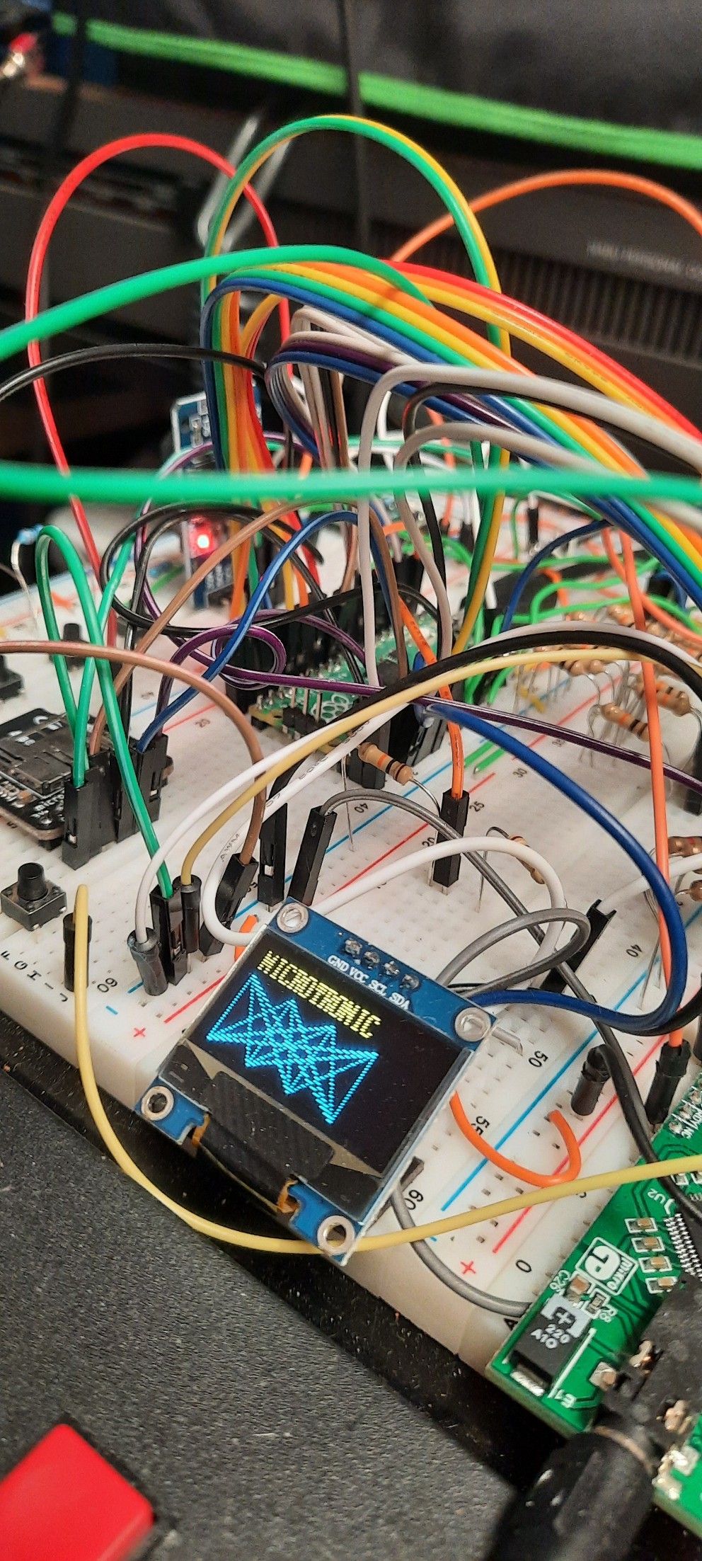
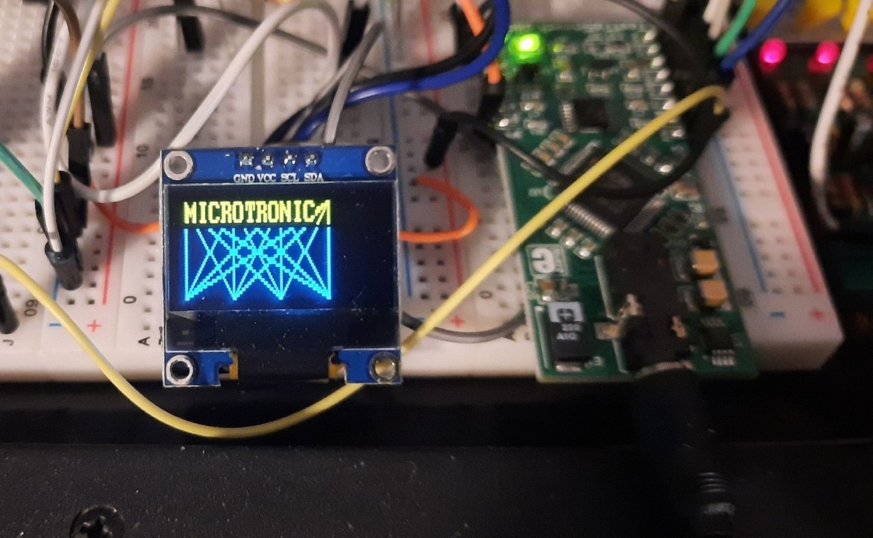
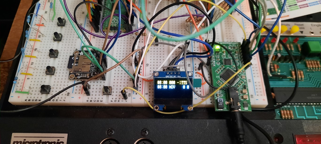
I've made some progress on the firmware - the SD card interface is now fully functional.
Also, the display font that came with the Pico C SDK SSD1306 OLED example was missing some characters, such as punctuation symbols. I substituted this font with another open-source font.
In the first line, the display is now showing the #bank number, followed by the address, then the 3 nibble op-code. The "-" indicates that op-code extensions are disabled; when enabled, it shows "*". Next, it either shows TTS or SND, depending on the position of the toggle switch. As mentioned earlier, I've exhausted the Pico's GPIOs and don't have enough IOs to support both sound and TTS simultaneously - at power-up, the toggle switch is used for selection.
The second display line shows the bank number, address, but mnemonics instead of the op-codes. The display mode can be toggled between 1) off, 2) only first line, and 3) first and second line (including mnemonics).
I have signed up for the RetroChallenge 2023/10 - my goal is to turn this into the multi-functional Microtronic extension I've been dreaming of. As described on the RetroChallenge page:
My goal is to create a multi-purpose expansion for the Busch Microtronic Computer (1981, 4bit). I already have a Raspberry Pico set up to emulate the Microtronic's 2114 SRAM. The Pico enables me to store and restore Microtronic memory dumps as files to resp. from SDcard, in milliseconds (the cassette interface takes minutes for a decent program!) By "snooping" the address bus and SRAM (which the Pico emulates), the Pico also knows the instruction currently being executed by the Microtronic. I can hence turn the Pico into a co-processor, adding new op-codes to the original Microtronic. I plan to add op-codes for OLED display output, sound, speech synthesis, a Real Time Clock, as well as bank switching. The goal is to have a working prototype at the end of the Challenge month that can then be turned into a PCB (consisting of a Pico, OLED display, loudspeaker and op-amp, SDcard, speech chip, and a few buttons for the user interface).
As much as I liked the clean look of the Pico Freenove breakout board, the scope of the project now calls for a proper breadboard with some real estate for the different components. This is my current kitchen sink prototype:
You can see it's lots of voltage dividers. In addition to the SRAM cables, there is one new jumper cable that grabs R12 from the board, as described in my previous log entry: https://hackaday.io/project/192655-picoram-2090/log/223457-i-know-what-you-are-doing Unfortunately, it requires a hardware mod to the Microtronic, but it is relatively clean as the single pin header is mounted to an existing via on the PCB.
Loudspeaker, push buttons, resistors, and a double pole 6pin toggle switch
The OLED display is controlled over I2C, and SPI is used for the TTS and SDCard. I was nervous if the SDcard and TTS would co-exist on the same SPI0 port, but luckily that turned out to be the case. Not sure about the RTC yet.
Obviously, a number of user interface buttons are required - since I am running out of pins, I decided to hook up a 5-button resistor ladder to one of the Pico's analog inputs. So it's only 1 pin instead of 5. The circuit (and following schematics) is from the well-known Arduino LCD & Key Shield (3.3V is used for the Pico though):
For sound output, I first looked at https://github.com/martinkooij/pi-pico-tone but had problems getting this to work. So I am simply using hardware PWM to generate sound. This is not as fancy as using the PIO (in pi-pico-tone), but works without bugging down the 2nd core as well.
I am already short on GPIOs - I have exhausted all of the Pico's IOs. For that reason, I cannot use sound and TTS simultaneously. I had to find a compromise, and choosing between either sound or TTS during start-up seemed like a reasonable compromise. A physical double pole 6pin toggle switch is used to toggle between TTS and sound.
As you can tell, I can either use GPIO 28 for resetting the TTS, or use it for sound output. I am using the double throw switch for routing; if the switch is in SOUND position, then the EPS_READY pin 26 is pulled high by the switch. The Pico firmware can determine the switch position during boot, and csn act accordingly (i.e., configure itself for TTS or sound). A few more GPIOs would have made this easier.
So, with the hardware and driver software fully operational, I am now in a position where I just need to grind away at the firmware!
I am now using the 2nd core of the Pico to drive the display, user interface, and implement the op-code extensions (as explained previously, extra op-codes for sound, speech, display, and memory bank switching), while the 1st core is constantly emulating the SRAM.
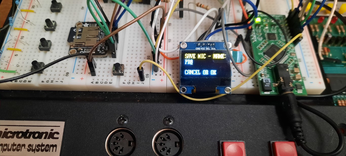
I have 5 buttons for controlling the expansion; from left to right:
UP, DOWN, BACK, OK, CANCEL
This should be enough to, for example, select files from SDcard, create file names, and control some other functions.
There is a main menu in which the buttons have to following functions:
UP: Load from SDCard
DOWN: Save to SDCard
BACK: Change current SRAM bank (16 banks)
OK: Extended op-codes ON/OFF
CANCEL: Change display mode (display off, address and op-code, address and op-code with mnemonics). In addition, the display also shows whether Sound or TTS is active, and if op-code extensions are enabled. Moreover, the current address is prefixed by the current bank number (0 to F).
By now, I have 8 Microtronic programs in the first 8 banks, and I can toggle through them with the "BACK" button. So banked memory works!
Next, I am going to implement the SDcard interface (storing the current SRAM bank to SDcard, and loading a memory dump back into the current bank from SDCard).
And then there is some work to be done for implementing the extended op-codes. Here is the table of the extended op-codes that I am planning to implement:
0xx ENTER DATA x
500 HEX DATA ENTRY MODE
501 DEC DATA ENTRY MODE
502 DISP CLEAR SCREEN
503 DISP CLEAR LINE <X>
504 DISP SHOW CHAR <LOW><HIGH>
505 DISP CURSOR AT LINE <X>
506 DISP CURSOR <X><Y>
507 DISP PLOT <X><Y>
508 DISP LINE <X1><Y1><X2><Y2>
509 SOUND OFF
50A SOUND PLAY NOTE <NOTE>
50B SOUND PLAY FREQ <LOW><HIGH>
50C SPEAK OFF
50D SPEAK BYTE <LOW><HIGH>
50E SPECIFY REG <REG>
50F LOAD VALUE FROM REG <REG>
70x SWITCH MEMORY BANK x
Alright Microtronic, I finally know what you are doing!
An additional motivation for this project is to make the Pico act as a co-processor - see, if the Pico knows the current op-code that is being executed (and the address / PC, obviously), I can make the Pico act on behalf of this op-code and implement "extra semantics" for some op-codes. What's "extra semantics" you might ask? Well, unfortunately, all 12bit op-codes are already occupied and already have a semantics in the Microtronic... but, some of these are "vacuous" and don't do anything meaningful - they are basically no-ops! For example, 0<x><x> copies register <x> onto itself. Same for "add 0 to register <x>", "subtract o from register <x>" - no Microtronic program is using these, and I can just grab them and give them extra-semantics to do something meaningful.
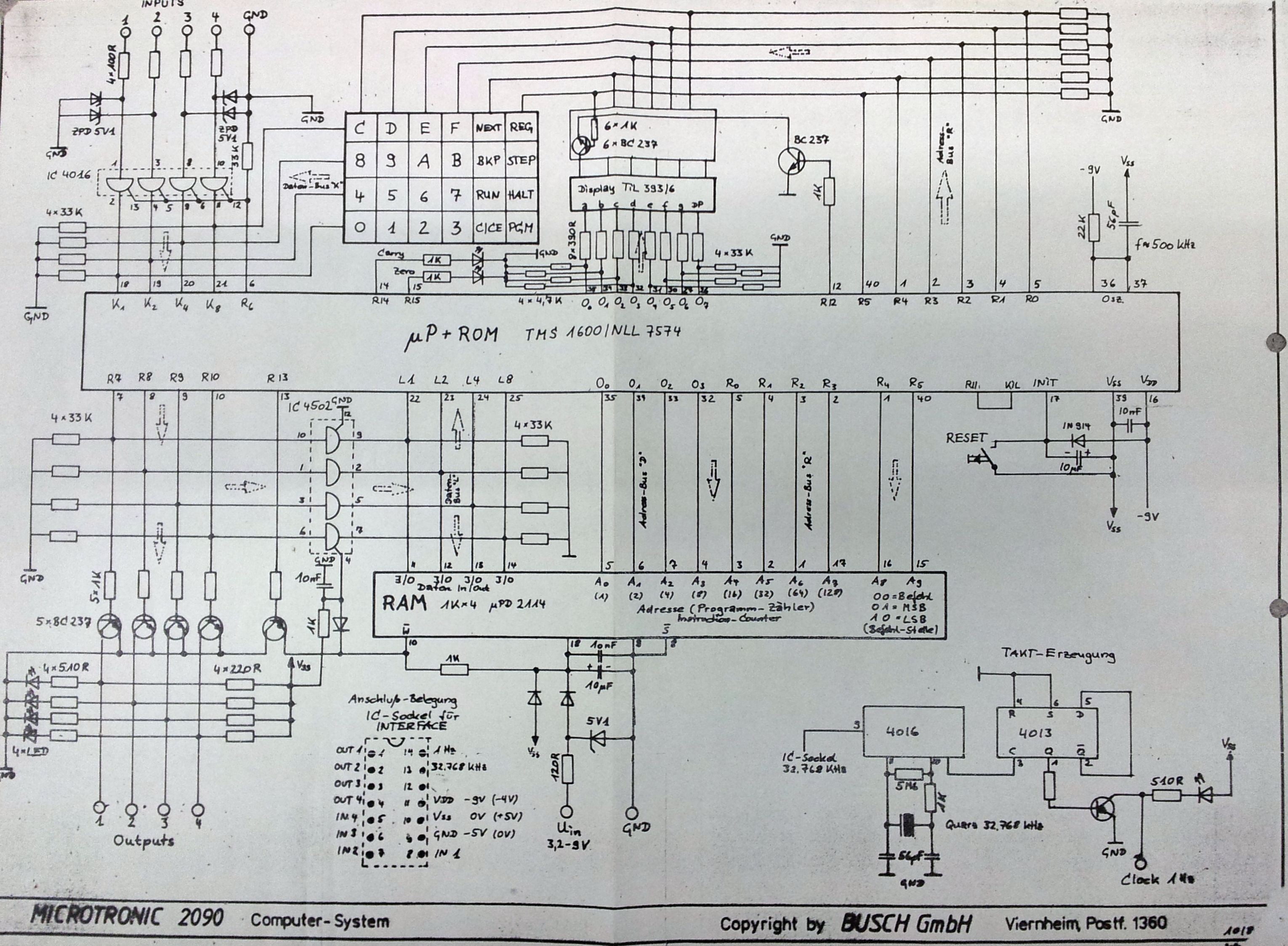
Looking at the schematics, we can see that the SRAM is addressed using the same GPIO lines that are also utilized for accessing the LED display and keyboard:
So how do we distinguish the SRAM accesses from all this additional activity on the GPIO "bus"? It took me many hours until I finally had a way of reliably detecting SRAM accesses.
A 12bit op-code starting at address <adr> is represented as follows in Microtronic SRAM: the first nibble is at <adr>, the second nibble at <adr> | (1 << 9), and third nibble at <adr> | (1 << 8).
My original idea was to simply implement a state machine that "tracks" the addresses as they show up on the bus: start in state 0, when <adr> arrives, go to state 1; when in state 1, and <adr> | (1 <<9) arrives, transition to state 2; when in state 2 and <adr> | (1 << 8) arrives, you have identified the SRAM access; reset to state 0. Right idea? Wrong!
The major problem with this approach is that the automata gets into wrong states - it is impossible to tell whether the transition from state 0 to state 1 is triggered by a real SRAM access, or by display multiplexing or keyboard scanning activities. Hence, the automata would sometimes get stuck, i.e., it transitioned into a wrong state and was waiting for a next adr pattern that didn't arrive as anticipated. I then thought, ok, let's reset the state when needed then (i.e., backtrack). But this strategy then had the problem that I would "miss" certain transitions, i.e., the automata wasn't getting stuck anymore, but when backtracking, I had already missed part of the address sequence. In addition to these "backtracking transitions" I then also started to incorporate timing-related info into the transition conditions, and things got more and more complicated, but I found no way of not "missing" certain addresses from wrong transitions and backtracking.
I had gotten myself into a dead end. Then I erased everything and started all over!
This time I had the right idea - I realized that I could only "retroactively" identify if an already presented sequence of addresses is part of the 12bit SRAM access pattern, but could not do so "proactively" (the automata approach had failed for this reason). I then simply kept a log ("sliding window") of the last four GPIO addresses: in addition to the current address in variable adr, I would also do a adr4 <- adr3, adr3 <- adr2, adr2 <- adr1, adr1 <- adr for each new recognized address change. By constantly scanning this window I then managed to identify the SRAM access with the following conditions:
if (adr4) {
  if (adr & (1 << 8)) {
    if (adr3 & (1 << 9)) {
       if ( (adr & adr3 ) == adr4) {
           // SRAM ACCESS FOUND!
       }
    }
  }
}
However, I also needed to add one more hardware-mod - by routing the R12 signal from the TMS1600 which is used for multiplexing the display segments over a transistor (see schematics above), I could also filter out all address patterns that would "light up the segments". Luckily, the Microtronic has a via for that signal, and I could simply solder in a pin from one of these breakout pin-headers, so I didn't need to disassemble the whole thing and it's also looking neat. A DuPont wire is used to route it into the Pico, again over a voltage divider. It took a bit of time again to find the right resistors for the divider, but in the end, I could now at least also exclude the "active" display accesses. I still don't have a way of excluding the keyboard scanning accesses, but that's ok. It works.
The only problem with the above condition / approach is that I cannot detect adr 0. But that's OK; it's a little bit ugly for program debugging, but good enough for op-code extensions (we just can't have an extended op-code at adr 00 then). It works for all other addresses. Sometimes, a fresh approach and change of perspective is needed in order to make progress!
I also added an OLED display to visualize what the Microtronic is doing, and utilized the 2nd core of the Pico to constantly refresh / update the display. First I tried using the same core that does the SRAM emulation, but this is no longer fast enough then (timing is critical here!). This is great for debugging! I'll also add mnemonics to the display soon.
Well, great, I can now implement the "Pico co-processor" idea!And easy thing to do is to arrange for the vacuous op-codes to perform extra-side effects. For example, "0<x><x>" can be intercepted by the Pico and it could, for example, mean "play note <x> on the loudspeaker". We have just added a sound op-code to the Microtronic! Or it can mean "send character <x> to the OLED display" - the Microtronic can now display text messages! I think the original designers might be surprised by this :-)
It's a little bit more complicated to implement op-codes that compute something that the Microtronic will then pick up. For example, imagine that the op-code "0<x><x>" means "calculate the square of <x> and write it to registers E,F". As the Microtronic is a Harvard architecture, I cannot write the 32 4bit registers ("Microtronic register file") with the Pico directly. SRAM is only for program memory, not for registers. But, I can inject a program segment with the Pico that, when executed by the Microtronic, will modify the register values to represent the computed value - "data as program"! Say the op-code "033" is detected by the Pico, now meaning "compute the square of 3 and write it to registers E,F!" If the current PC is adr, then the Pico will now first compute the square of 3, and subsequently, starting from adr+1, "inject" a sequence of MOVI (Move Immediate, i.e., move a constant to a register) instructions that write the Pico-computed values (0 and 9) to the appropriate registers (E and F). Hence, the Pico will present 10E at adr+1 to the Microtronic, and 19F at adr+2. The Microtronic will execute these, and the Pico-computed values will appear in the appropriate registers. At adr+3, the Pico will present a JMP / GOTO to adr+1. After the Microtronic has execute this last JMP / GOTO, the Pico continues presenting the original program from SRAM to the Microtronic again. The "injected" program sequence has been executed, and the Microtronic continues execution of the original program as usual. But has now the computed square 09 in its EF registers. Magic!
Next, I am going to work on the SDcard for SRAM images.
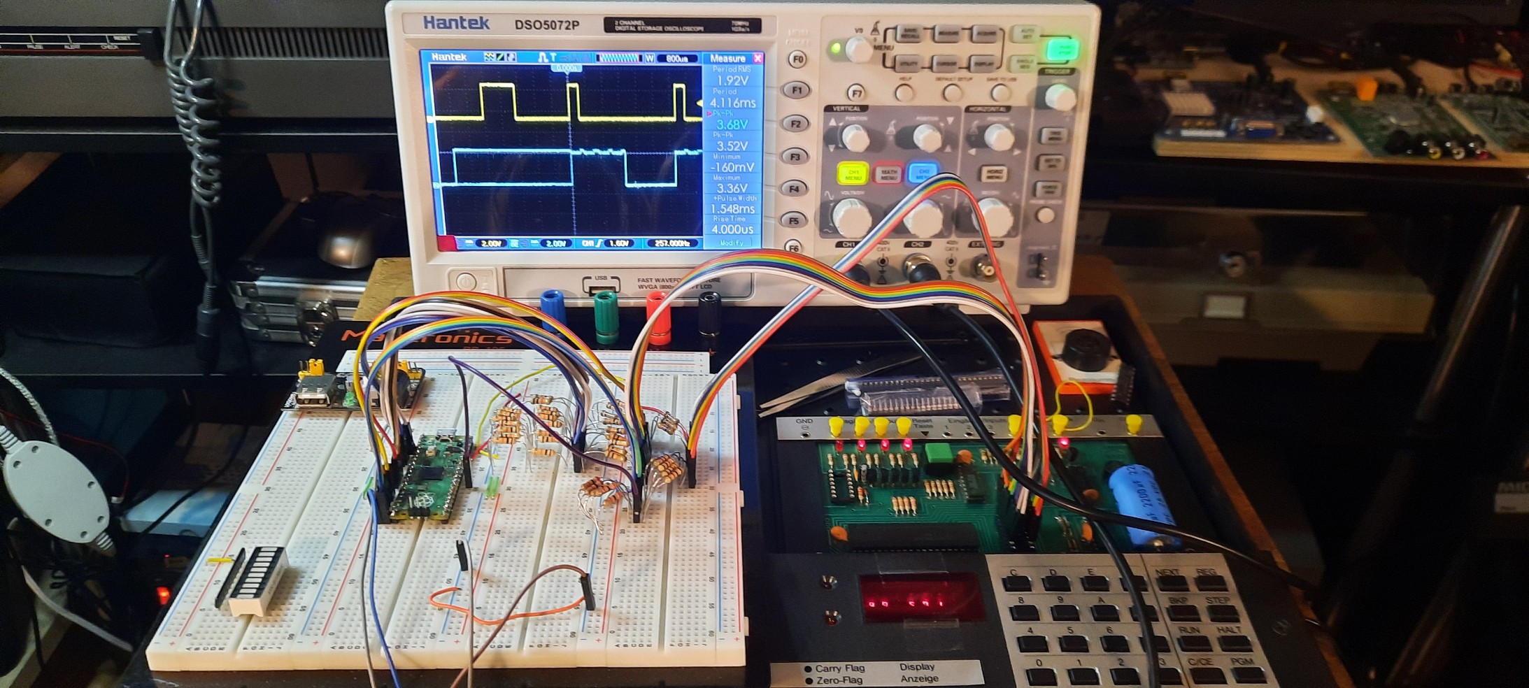
Feeling better now - no more > 5 V peak-to-peak levels. On display is address bit A0 and data bit IO/1. Both are now at ~ 3.4 V; the mean is much lower. I was surprised about the 200 Hz frequency... this is probably misleading though and probably caused by the LED display refresh and keyboard scanning activities that are performed over the same TMS1600 GPIO lines. But then, the Microtronic is not the fastet: 500 kHz clock, and after all, it's an emulator that is running in there in the firmware, not native TMS1600 machine code. I believe that SRAM access frequeceny is more in the 1 -2 kHz range.
 Michael Wessel