Ted Yapo
-
Leaded version with feedback
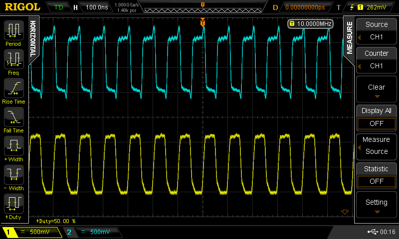
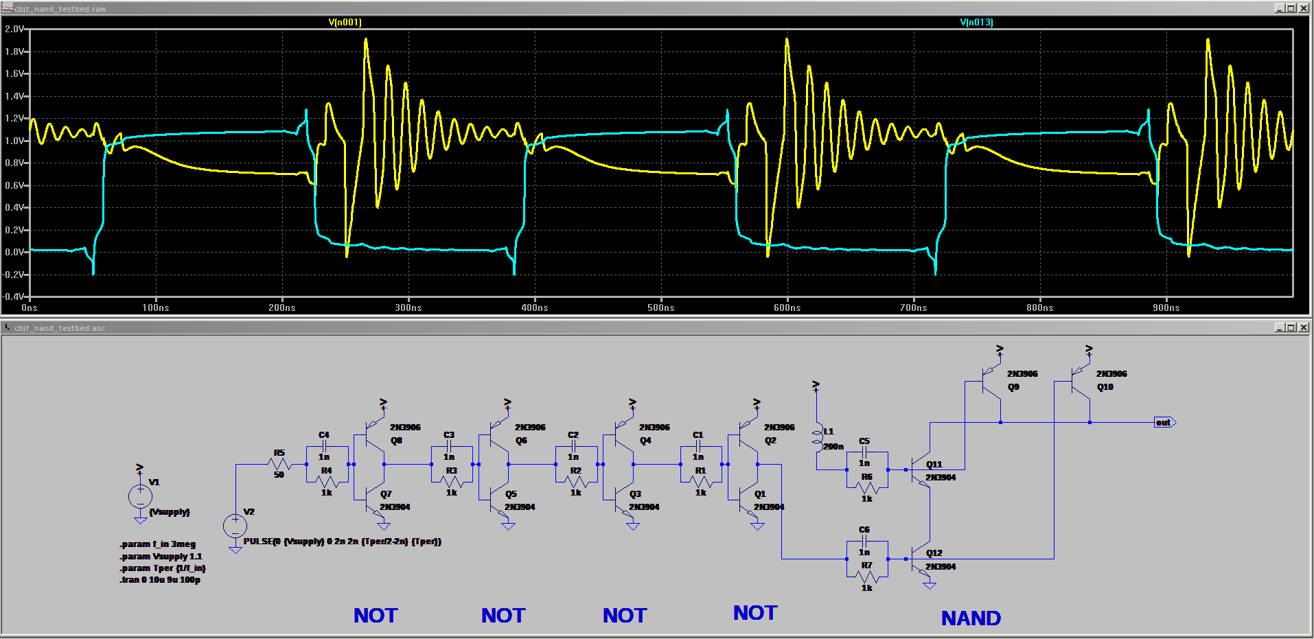
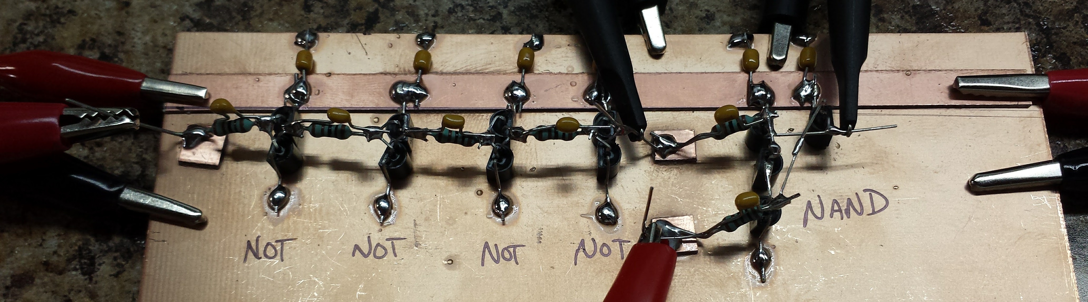
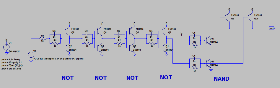
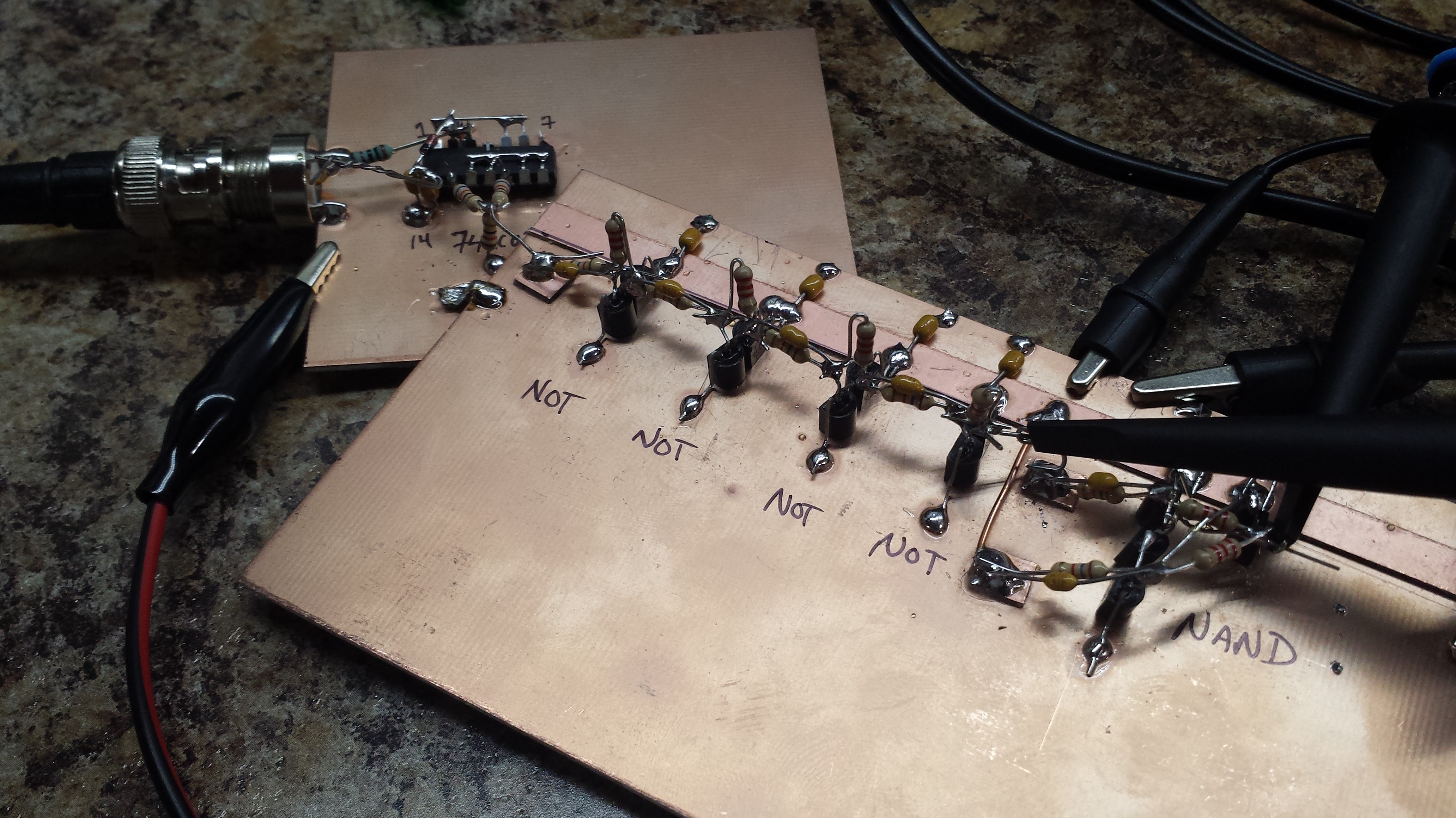
01/29/2017 at 01:41 • 3 commentsI soldered together a test using through-hole 2N390{4,6} transistors and 1.6k input / 2.2k feedback resistors. This test included four inverters driving either input of a NAND gate (also made with 2.2k feedback resistors):
![]()
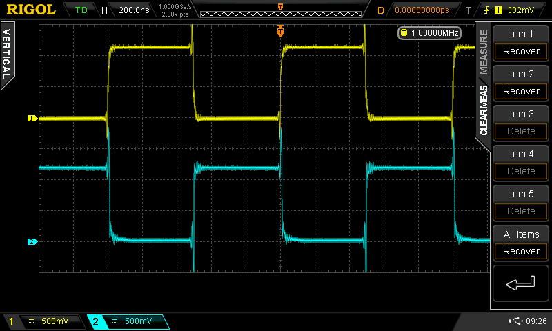
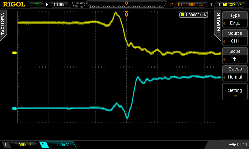
I tested this the same way I had done the SMT version: using a level/impedance/edge rate converter to drive the input with brief (~20ns), isolated (~100 kHz) pulses of either polarity. Like before, one of the output edges is delayed relative to the others, and this delay drops with input pulse length. I decided to use single, short pulses (about 24 ns after the inverter chain) to measure the NAND gate delays. This corresponds to a single pulse of a 21 MHz signal, so these results should be valid for systems clocked at this speed or below - and you can ignore the variable delay; this is a worst-case.
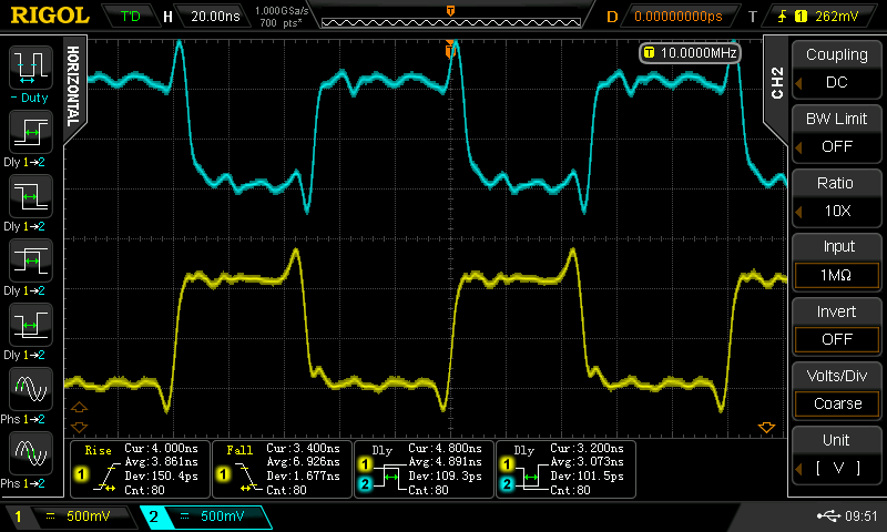
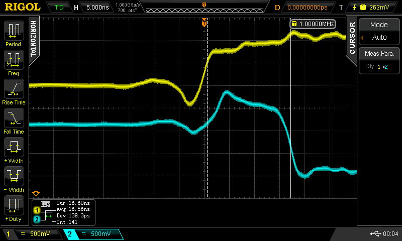
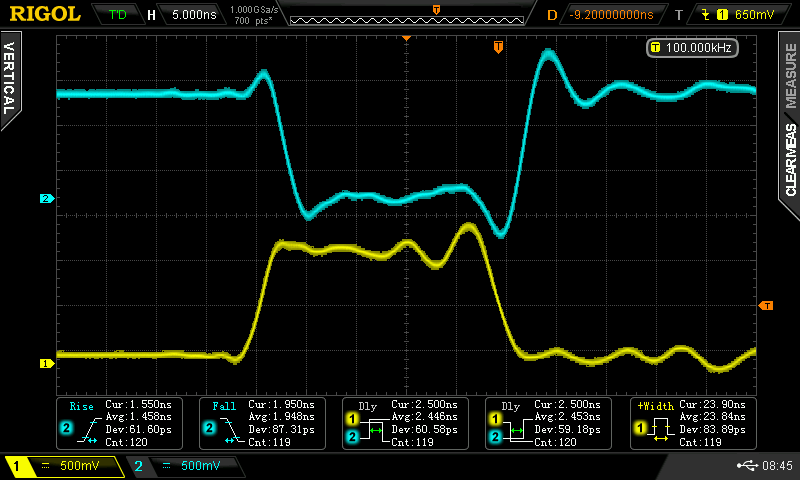
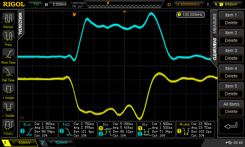
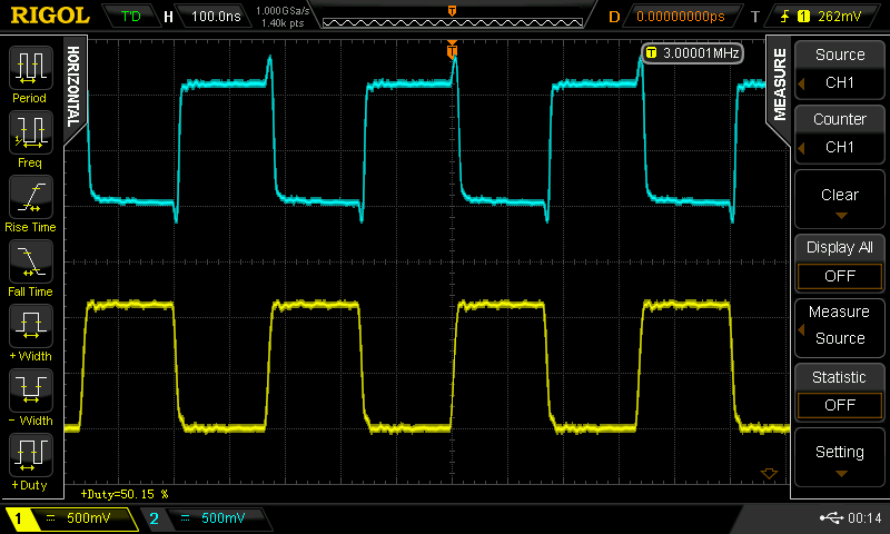
Upper Input Driven
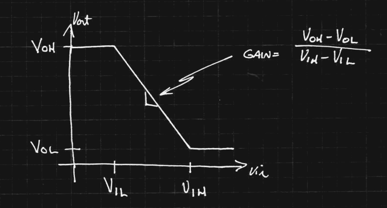
With the lower input tied high, and the upper input driven, I observed the following waveforms (yellow = input, cyan = output).
![]()
![]()
The rise and fall times vary from 1.5 ns to 3ns. These are fast edges and would require some thinking about long wires or traces in a system using these gates. With the positive input pulse, the two propagation delays are equal at about 2.5 ns. With the negative input pulse, one propagation delay is 1.5 ns (the output rising edge), and the other is 5.4 ns (the output falling edge).
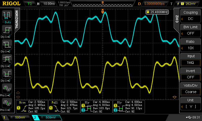
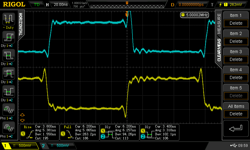
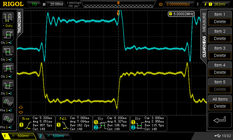
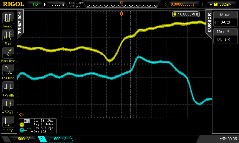
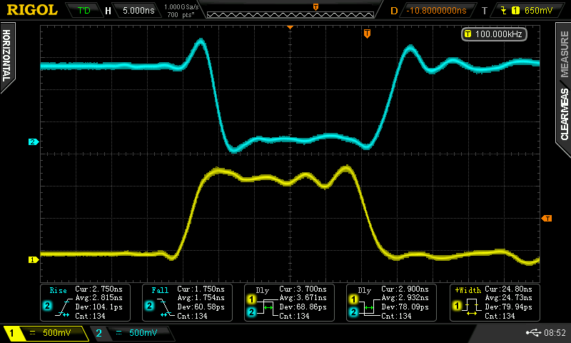
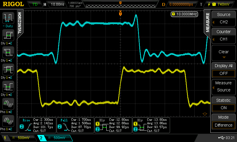
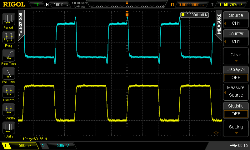
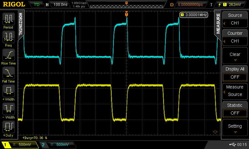
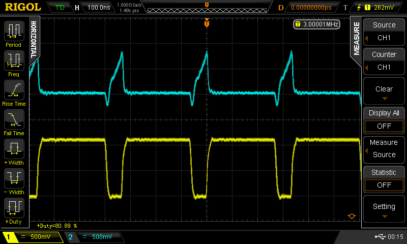
Lower Input Driven
![]()
![]()
Here, the rise and fall times are longer, ranging from 1.8 ns to 3.9 ns. With the negative-going pulse, we see delays of 2 .0 and 7.2 ns. With the positive-going pulse, the delays are 2.9 and 3.7 ns.
The 7.2 ns is the worst case of any observed - this is really the number you should think about to evaluate these gates. If you were building a small module, maybe a flip-flop or counter, you might be able to take advantage of some of the faster delays instead of simply assuming 7.2 worst-case. Generally 7.2 seems to be the number, assuming the minimum pulse widths in the system are 24 ns or more - corresponding to a system clock of 21 MHz or less.
I think the take-away from this exercise is that the feedback resistor solves the problem with isolated pulses. There are probably ways to improve things, including splitting the input resistor like was published in the 1950s. I might leave it at this, though.
Well, maybe one PCB for a counter or something, since I have the SMT transistors, and the R's and C's are dirt cheap.
-
Feedback Version Tests
01/22/2017 at 17:39 • 3 commentsI hadn't home-etched a board since I discovered OSH Park (first order 1/12/13). Actually, before that, I used another service that didn't do soldermask or silkscreen, only offered one size board, and made you use their proprietary layout software. I also walked to school - uphill both ways; kids these days have it easy. Anyway, my bottle of ferric chloride is at least five years old, but it still works:
![]()
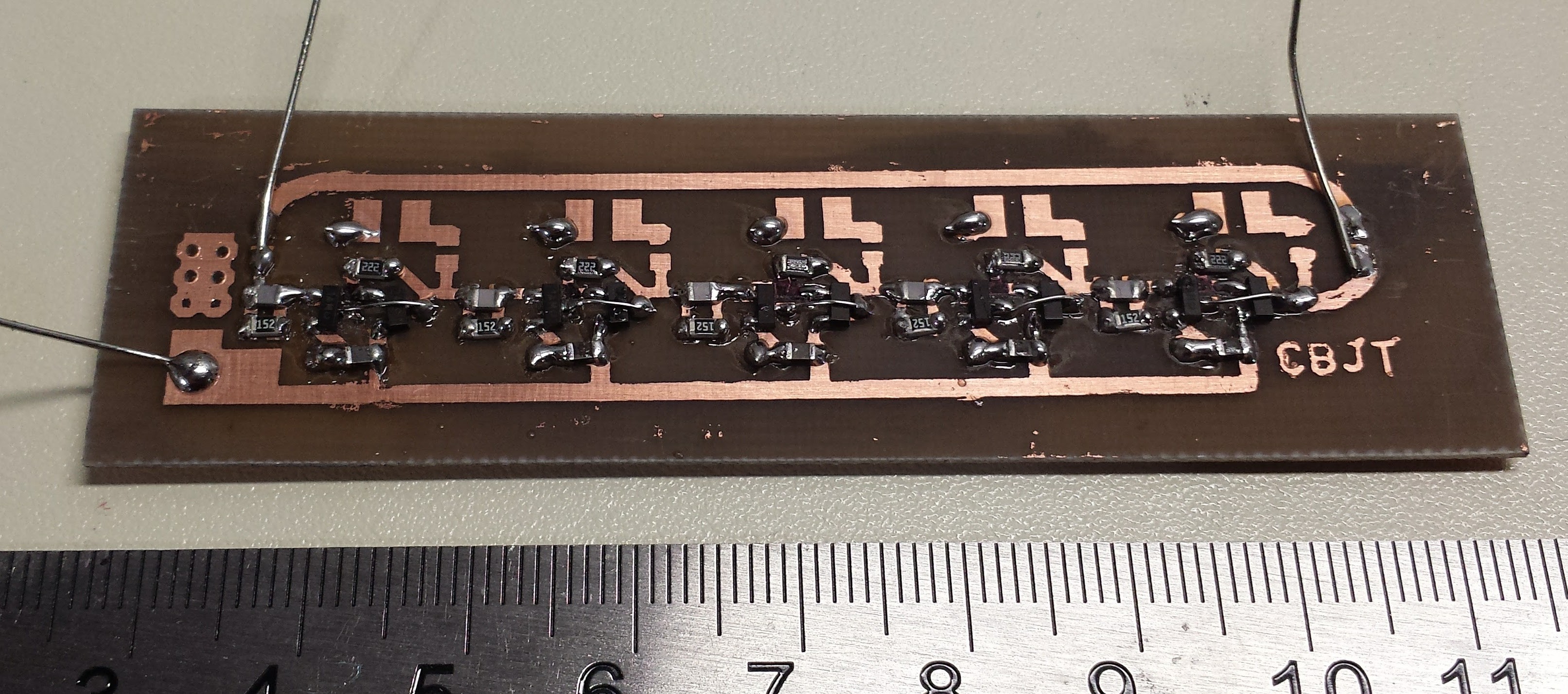
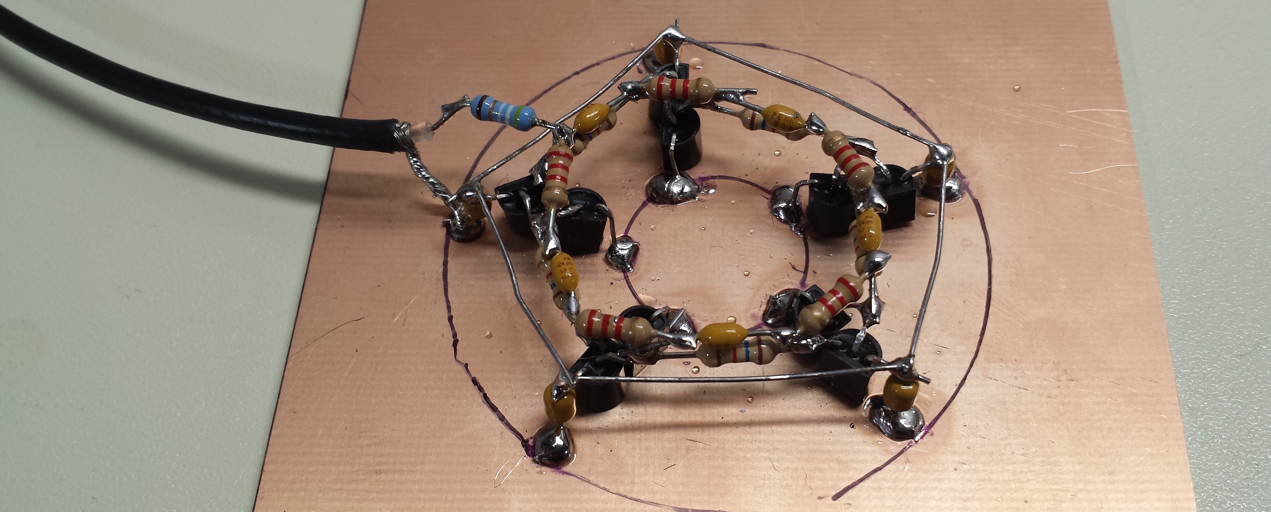
It's a 5-stage ring oscillator with MMBT3904/MMBT3906 devices and the 2R (feedback) design. I didn't have 1.6k 0805 resistors, so it uses 1.5k and 2.2k. The bottom of the board is solid copper, and ground connections are made with wire "vias" in drilled holes. At 1.2V supply, the thing runs at 30.3 MHz, indicating a propagation delay of 3.3 ns. This is significantly longer than the simulations, but not really that bad. I don't think the 1.6k -> 1.5k substitution is to blame; it didn't make much difference in the simulation - but it might be causing other issues described below.
Thinking there might be something wrong, I built a version with through-hole parts, too:
![]()
This one uses 1.6k resistors. It runs at 33.4 MHz, for a propagation delay of around 3.0 ns at 1.2V. If you turn up the voltage, you can get it to peak around 37MHz, at high current drain. At high enough voltages, the speed drops again. I can't explain the difference in speed between the two versions. The TO92's are bona fide Fairchild transistors from a reliable distributor; the MMBT's are no-names I (probably) bought on ebay. Maybe they're not the real thing? Of course, this could be layout issues, too - is that long feedback line to blame? I think it's only about 250ps long electrically. And those 1.5k R's? Hmm.
Pulse Testing
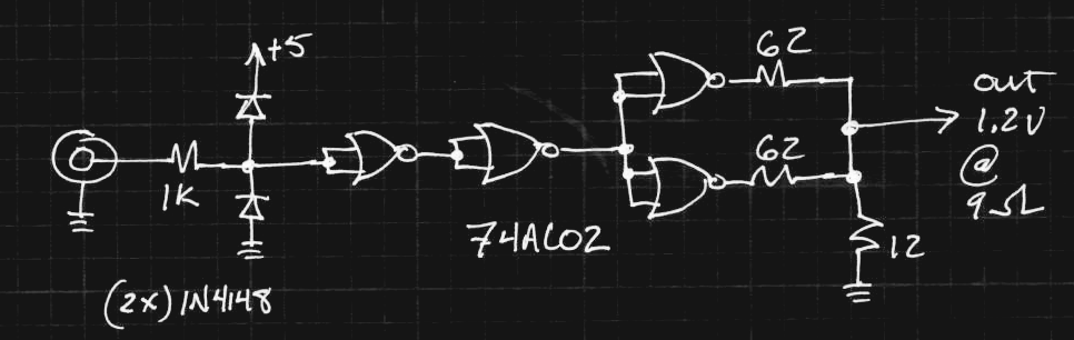
Since the output impedance of these gates is so low, and the edge rates so fast, the output of my 50-ohm signal generator isn't a good source for testing. I decided to build a buffer with a 74AC02 quad NOR (because I have a ton of them). The edge rates of the AC logic are around the same as I have seen with these CBJT gates, and I made a voltage/impedance converter network so that the output is around 1.2V peak with a 9-ohm impedance:
![]()
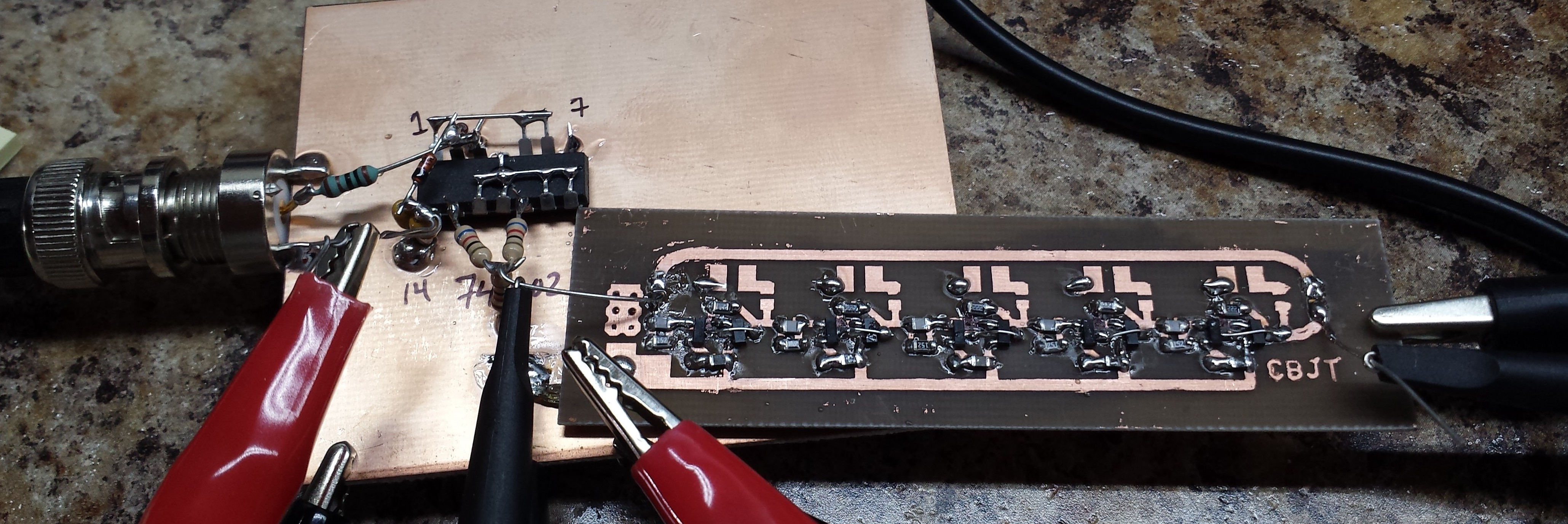
This circuit assumes a 5V supply for the 74AC02 and a 12-ohm output impedance for these NOR gates - I had previously measured around this value. Using this circuit at the output of my signal generator produces waveforms that look like the output of the CBJT inverters. Here's the adapter soldered together with the SMT test circuit:
![]()
First Impressions
So, I fired up a 10 MHz square wave input, and measured the output at the end of the chain of 5 inverters (with the ring oscillator feedback trace disconnected). Here are the waveforms (yellow = input, cyan = output):
![]()
The rise time is about 2.1 ns, and the fall time 1.5 ns: fast edges. The measured propagation delay is 2.7 ns on average. This is faster than the ring oscillator measurements. You can also see that my generator at 50% duty cycle doesn't appear to be exactly 50%. Maybe the 74AC02 converter is stretching one side?
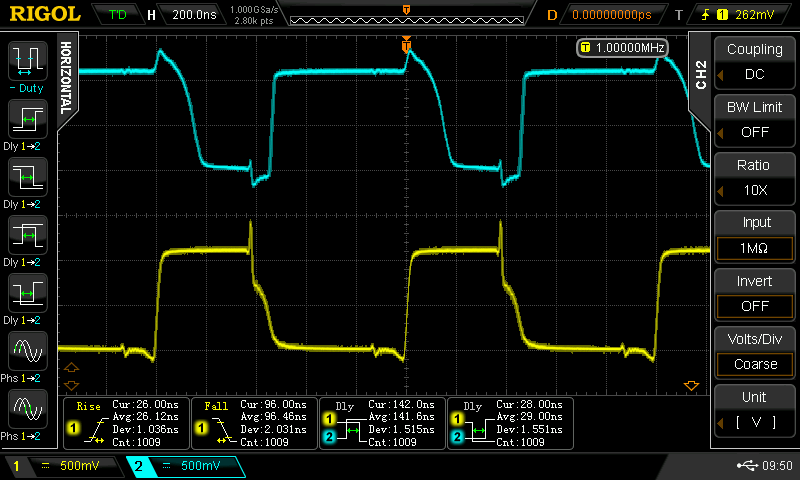
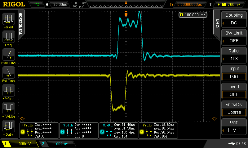
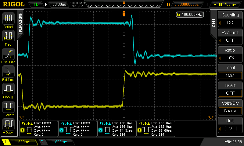
Changing Duty Cycle
The non-feedback design had a problem with transistor saturation at high or low duty cycles. This version has its own peculiarities, namely it stretches isolated pulses. As before, a 50% duty cycle input is fine, but isolated pulses are distorted a little. In this case, the pulse (either high-going or low going) is stretched by an amount inversely proportional to the pulse width - very counter-intuitive. For example, here are input pulse widths of 18.5 and 133ns producing output pulses of 31.3 and 137 ns:
![]()
![]()
This is a stretching of 12.8 ns for the shorter pulse and 4 ns for the longer one. Bizarre. This happens for negative-going isolated pulses, too. And, it goes away with near-50% duty cycles, like before. It may be that this would be improved if I had 1.6k resistors in there instead of 1.5. I can try later with through-hole components where I have a stock of the 1.6k.
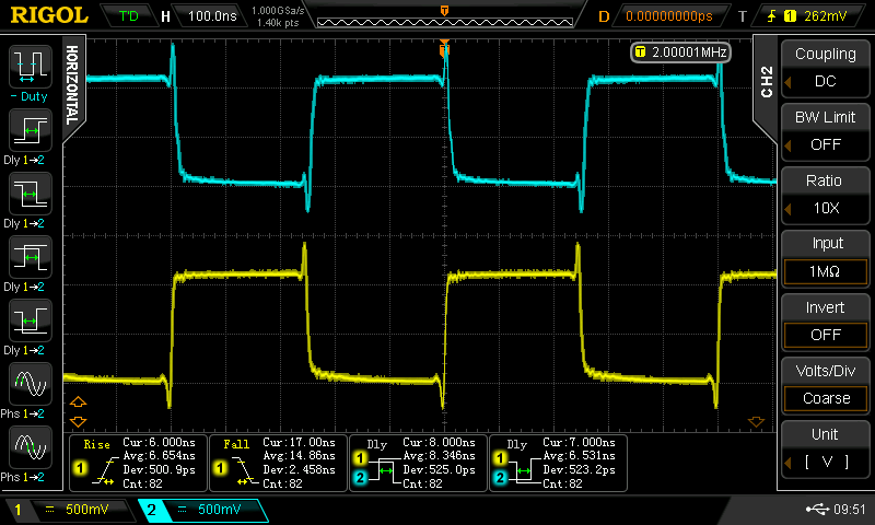
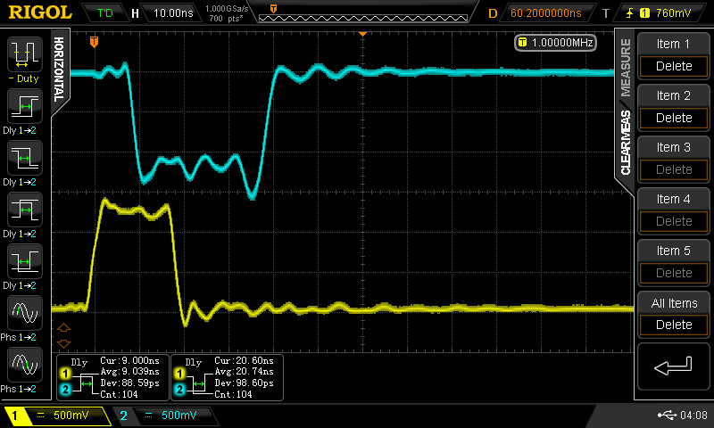
One way to look at this pulse stretching is as an additional delay. If you account for th worst-case stretch as part of the propagation delay, your design should just work. Here's that this looks like (with positive pulses this time):
![]()
![]()
On the left, with a 20 ns input pulse, the worst case delay here is 21ns for 5 inverters, or 4.2 ns each. This pulse represents a single clock pulse in a system with period of 40 ns, or 25 MHz clock frequency. With a 100 ns input pulse (right), the delay has decreased to 2.7 ns, matching the measurement with the square wave.
It's almost like there's a minimum pulse width for the output. I collected the following data for input pulse vs output pulse width:
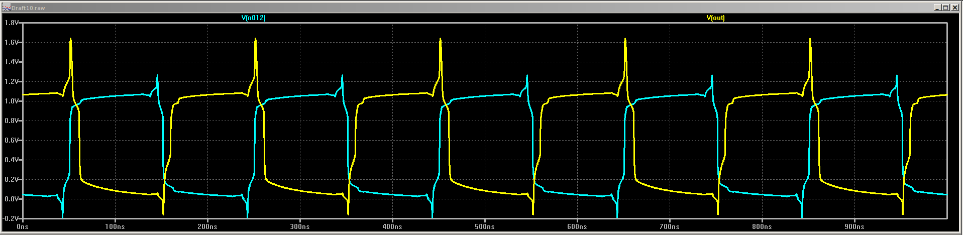
Input Pulse Width (ns) Output Pulse Width (ns) 18.54 31.3 28.22 39.05 44.80 53.63 52.81 60.88 60.90 68.23 68.86 75.60 84.90 90.62 92.91 98.24 100.9 105.9 108.9 113.6 116.9 121.3 132.9 136.8 This data looks pretty linear when plotted. A simple regression line gives:
So, it's almost like there's a minimum output pulse width of 12.5 ns for isolated pulses. But, the stretching is reduced for longer input pulses (that 0.927 should be 1). Very strange.
I'm not sure what to make of all of it yet. Maybe moving to the 1.6k resistor will improve things? And what about 2-input gates, NAND and NOR? More things to look at.
Full Circle
So, I'm finally coming to understand why the original design we found uses a split input network and pull-up/pull-down resistors. I've been playing with some simulations, and it looks like this buys you some nice properties (less sensitivity to power supply level, higher gain, easier control of saturation) but at a price of more components and possibly another supply rail. A wiser person might have adopted that design first, but I had to bang my head against this problem until I understood how they ended up where they did. I think I'm getting close - sounds like another log is in my future.
-
2N390x CBJT Logic
01/21/2017 at 03:10 • 17 commentsI think I've tweaked the component values into something possibly usable. The feedback resistor seems to improve the speed tremendously - by keeping the transistors out of saturation - at the cost of greatly reduced gain. But maybe we don't need that much gain? Here are the latest component values:
![]()
the feedback resistor is new. It keeps the voltage on either base away from the rails to prevent either transistor saturating. An unfortunate side effect of this arrangement is a greatly reduced gain - at DC, the gain is approximately the ratio of the two resistors 2.2k / 1.6k = 1.375. Yes, this is very small - I thought it would be too small to be useful, but maybe it's OK, if you're careful. To get a feel for just how small this is, here's the voltage transfer function, which would normally be a sharp step function for an inverter:
![]()
For most of the input voltage range, this is a linear amplifier. It's only at the extremes that it starts to look like a logic gate. But, since the output stage is symmetrical and low-impedance, and the input stage high-impedance, maybe this is enough gain to build logic circuits. Theoretically, you only need a gain of 1 after any losses...
Then again, consider the speedup capacitor. At 10 MHz, that 100 pF capacitor has an impedance of about 160 ohms, so the gain is now around 14. That doesn't sound so bad.
I built an early hardware test (with different RC values) of a ring of inverters with feedback resistors. At 1.1V supply, they were happy to just sit there and bias themselves to 1/2 the supply without oscillating - the gain was too low. At 1.2V, they always started ringing, and once started, they kept going as the supply was turned down to about 0.7V. So, I started simulating things at 1.2V instead of 1.1. The final supply voltage will probably need a tuning knob.
Speed SimulationsThe original problem from a few logs back was that the logic worked well with high-speed square waves, but not at low or high duty cycles. I'm convinced now that rapid switching was keeping the pair out of saturation. A short pulse after a sustained high or low input wasn't enough to pull one of the pair out of saturation. The added feedback resistor holds the base voltage close to the midpoint, keeping both transistors out of saturation. This allows the gate to respond to brief, isolated pulses as well as waveforms with high repetition rates. Here's a test waveform at the input and output of a chain of 10 inverters:
![]()
The measured delay for 10 inverters is around 16 ns, or 1.6 ns per inverter. This is significantly faster than what I had seen before. I haven't constructed any of these inverters yet, so I can't be sure it will work with real components. The initial low period above is a test for the saturation problem. Without the feedback resistor the PNP saturates on the initial stretch, and we get this - no output at all:
![]()
I suspect the output would eventually start switching because this is only a 5 MHz square wave, but I didn't let the simulation run that long.
Fan-out Test
In this simulation, the second-to-last stage drives a fan-out of 10 inverters.
![]()
This slows down the trailing edge of the first pulse so that it happens at a 31 ns delay (instead of 16 ns with the simple inverter chain). With a fan-out of 5, the delay is 24 (as opposed to 16) - so maybe a rough rule of thumb is that fan-out is roughly equivalent to cascading stages. It looks like driving 2 inputs delays the signal about as much as chaining 2 inverters. If the delays were all due to RC effects, this would be the case. This is not great, but might be acceptable. Again, I haven't measured this on the hardware yet.
In any case, increasing fan-out decreases switching speeds. You see this with CMOS logic where the input capacitance of added driven inputs slows down the transition speeds. Although with integrated CMOS families, the effect is not this pronounced.
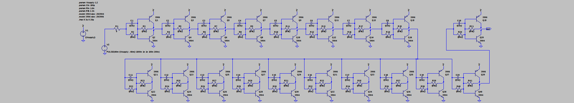
Input/Output Impedance
I roughly estimated the output impedance of the stage at 9 ohms. The input impedance is above 1.6k until about 350 kHz, then drops to about 200 ohms at 10 MHz. The vertical axis is labeled in volts because I used an AC current source to probe the input impedance.
![]()
I won't paste plots here, but these gates drive 50 or 100-ohm terminated lines just fine. I tested outputs with split-terminations of 100 ohms to ground and V+ (for 50 ohm lines) and 200 ohms to each (for 100 ohm lines). No problems at all, which is what you'd expect from under 10 ohms output impedance. With fast edge rates, you might have to use terminated lines to maintain signal integrity. Of course, you can also source-terminate transmission lines, but you can't fan-out and source terminate (unless your transmission lines are exactly the same length). I didn't look at how many split-terminated loads you can drive - but at least (2) 100-ohm loads, since you can drive (1) 50-ohm load.
NAND Gate
These component values translate straightforwardly into the NAND design:
![]()
In simulation, the upper input shows a delay of about 2.3 ns, and the lower input shows about 3.6 ns. It may be possible to balance these somewhat by tweaking the component values a little, but I haven't had a chance to try yet. Like the inverter, the NAND has no problem with saturating during long periods of stationary input values; the feedback resistor has cured the mysterious square-wave illness.
Next Steps
I need to build some of these gates from actual components and see if they perform as well as the virtual ones. The low DC gain of these stages troubles me a little, but I think the logic is still workable.
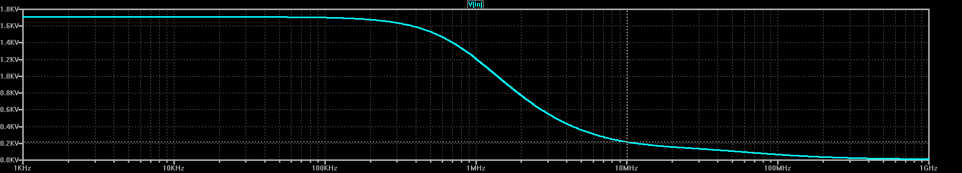
UPDATE 20170121 : How much gain is actually required?
I was a little hesitant at first about the low gain of these gates. Then I started thinking about the minimum gain that would be required to meet commercial CMOS family specs. Here's what a worst-case (lowest gain) transfer curve would look like that still meets the Vih, Vil, Voh, and Vol specs from a datasheet:
![]()
For the 74HC04 at 6V supply and with all worst-case values, we get (5.2 - .4)/(4.2-1.8) = 2.0. At a 2V supply, it's (1.9-0.1)/(1.5-0.5) = 1.8. Hmm, maybe 1.375 isn't that crazy after all.
-
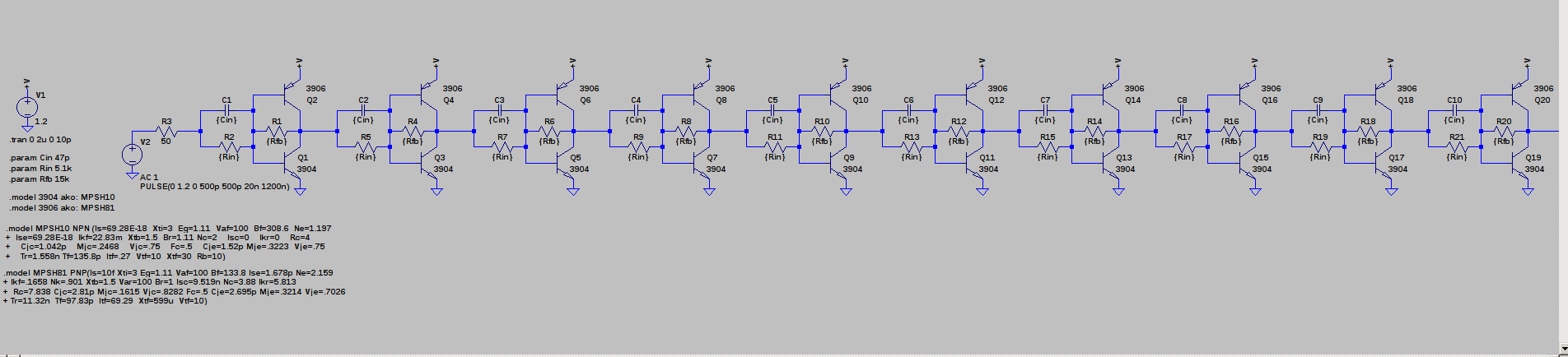
MPSHxx Teaser: would you believe 500ps?
01/20/2017 at 18:18 • 17 commentsI shouldn't post this yet; there's surely some catch that will prevent you from going this fast. But, I'm doing it anyway. One of my favorite NPN/PNP pairs are the MPSH10 / MPSH81 RF transistors. Obsolete in TO92 now (although I have a thousand or so kicking around), they're still available in SOT23 as MMBTH10 / MMBTH81. With an ft of 600+ MHz, this pair is twice as fast as my other "fast" favorites, the 2N3904/2N3906 (300 MHz ft). Anyway, I couldn't help but simulate some CBJT inverters with the RF pair. Here's the input to, and output from a chain of 10 inverters. One edge is delayed by 3.6ns, the other by 5.0 ns. That equates to a propagation delay of under 500ps per inverter. Pretty fast.
![]()
Here's the circuit. It might be difficult to find in the parameters, but the input resistor is 5.1k, the speedup capacitor 47p, and the feedback resistor 15k. The power supply is 1.2V.
![]()
If you want to play around in LTspice with this, I've uploaded the simulation file. I haven't even simulated a 2-input gate yet, so that may or may not work. I also haven't built one of these yet. Even testing it may provide some unique challenges.
I am still working on choosing the R's and C's to optimize the 2N3904/2N3906 pair. I started with a 1k input resistor because I have a giant reel of them from a late-night ebay purchase years ago. This is perhaps not the best objective function for optimizing the design :-) So, I'm having a close look at the R's and C's, considering speed, power, fan-out, etc, and then testing on hardware to make sure the simulations didn't lie. It's going to take a little while longer.
UPDATE
I ran a 5-inverter ring oscillator simulation with these transistors. This makes it look like actual propagation delays are closer to 1 ns. I still have no idea if these speeds will be achievable in reality.
-
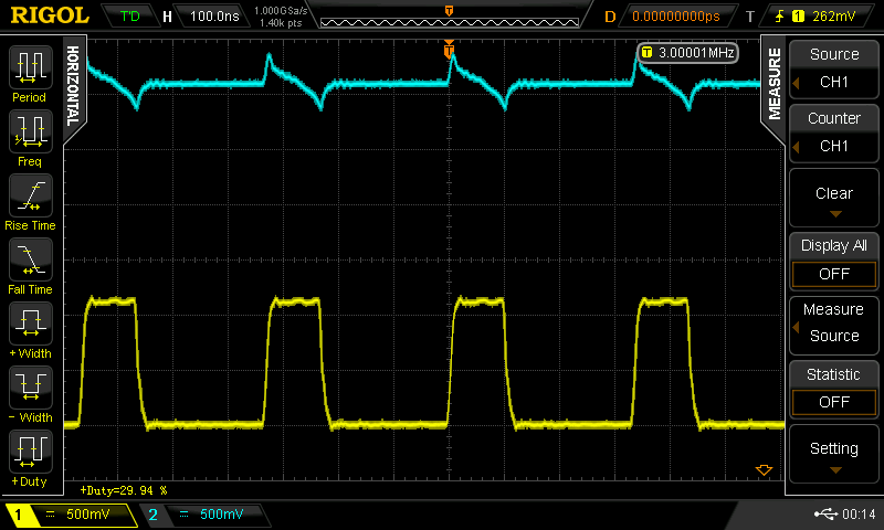
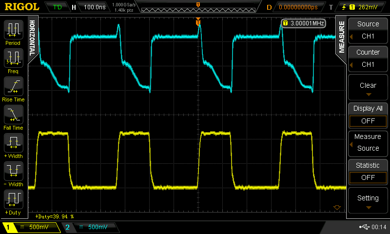
No, it's not that fast
01/18/2017 at 16:32 • 29 commentsI stayed up pretty late looking at this stuff - it just didn't make sense. Finally, after playing with the simulations, I found something. The complementary NPN/PNP pair can switch very fast if it is switched continuously - like with a 50% duty cycle pulse. This somehow keeps both transistors biased, or keeps them out of saturation, or something, that allows them to switch very quickly. After a period of time this "magic quality" wears off, and they switch slowly again. I don't have a full explanation yet, but I've seen it in simulation and on the hardware now. I started with the simple inverter circuit again: here simulated with 1 nF and 100 pF caps:
![]()
when you drive the 100 pF cap version with a 50% duty cycle square wave, you can get it to go 25 MHz (the limit of my current testing setup). With duty cycles other than 50%, the waveforms fall apart. Here are some scope shots for a 3 MHz input with various duty cycles. Yellow (lower trace) is the input to the inverter; cyan (upper trace) is the output.
![]() 30%
30%
![]() 40%
40%
![]() 50%
50%
![]() 60%
60%
![]() 70%
70%
![]() 80%
80%
This is not just a case of minimum pulse widths - for example, here's the same circuit driven at 10 MHz with 50% duty cycle. The high time and the low time are both shorter than the 30% and 80% duty cycles above, but there's no problem at all with the output:
![]()
The same thing happens with the 1 nF capacitor, just at different frequencies. This effect is also present in the ring oscillator, which naturally assumes around a 50% duty cycle, so it is able to oscillate very quickly.
Something is happening in the transistor pair that I don't understand. I don't think the effect is really due to the duty cycle - I suspect that a recent pulse makes the pair faster for a period of time. If another transition happens within this window, the pair will remain fast. Once the effect has worn off, the pair will be slow for the next transition. I can't fully explain what is happening inside the transistors yet, but I see the same effect in LTspice, where it's much easier to make measurements, so I have a shot at figuring it out.
The real bummer is that this invalidates all the previous speed testing. I haven't fully re-run the tests yet with isolated pulses instead of square waves, but a quick look at the scope puts the propagation delays in the 25-35ns range. It's not quite as bad as a CD4001, but it's no match for even the 7404.
-
Looking for the Goldilocks capacitor
01/18/2017 at 02:30 • 4 commentsUPDATE: the speeds measured here don't represent the true switching speed of these gates. See this log for more details.
I initially settled on 1 nF speedup capacitors because they seemed to perform better in simulations - which were done with lower-frequency signals. The value did seem large at the time, but it seemed to work OK in practice, even though the ring-counter simulation would go much faster with smaller capacitors. I finally got around to trying smaller capacitors on the real hardware. With 100pF caps substituted for the old 1 nF's, everything goes more than twice as fast (with a catch, discussed below). The ring counter went from around 10 to 25 MHz:
![]()
This frequency implies an average propagation delay of 3.92 ns. The scope measures 4.0 and 4.9, but may be confused by the under/overshoot. In any case, it's more than twice as fast as the previous circuit which had around 9.5ns of average propagation delay. A 74AC04 inverter has a typical propagation delay of 3.5 (TPHL) or 4.0 (TPLH) ns. This silly CBJT logic has gone from 74HC speeds to 74AC. Or so it would seem.
What's the catch?
Knowing my luck, there has to be a problem somewhere. It didn't take long to find it, either. At lower speeds (when driven with the signal generator), the waveforms fall apart - I saw this behavior in the simulations, too, which made me think larger caps were necessary. For example, a chain of inverters driven with a 1 MHz squarewave looks terrible (below, left). The same inverters look fine with a 2 MHz input (below, center), and OK to the top of my generator at 25 MHz (10 MHz shown below right) - some of that ringing is the ground leads on the probes; I was too lazy to solder on Z0-probes.
![]()
![]()
![]()
100 pF just isn't enough at lower frequencies, which is bizarre, because it should be all about edges. Did I screw up and have the DDS set for a sine wave output?? Is the DDS edge rate lower for lower frequencies? Now I'm going to have to re-check when I get a chance - maybe this is something simple. It would be convenient if this bizarre behavior at low frequencies just went away :-)
And the NAND?
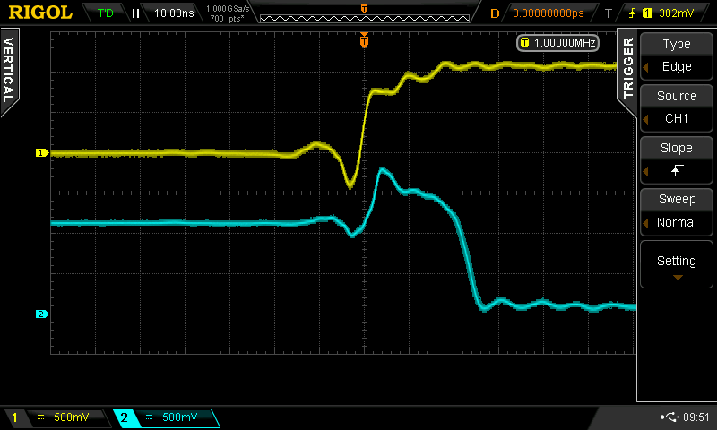
The NAND gate performance was also improved with the smaller capacitors - at least for higher frequencies. Driving the lower input showed a 3.3 ns TPLH and a 6.3 ns TPHL (the 74AC00 has 6.0 and 4.5 ns at 5.0V, respectively):
![]()
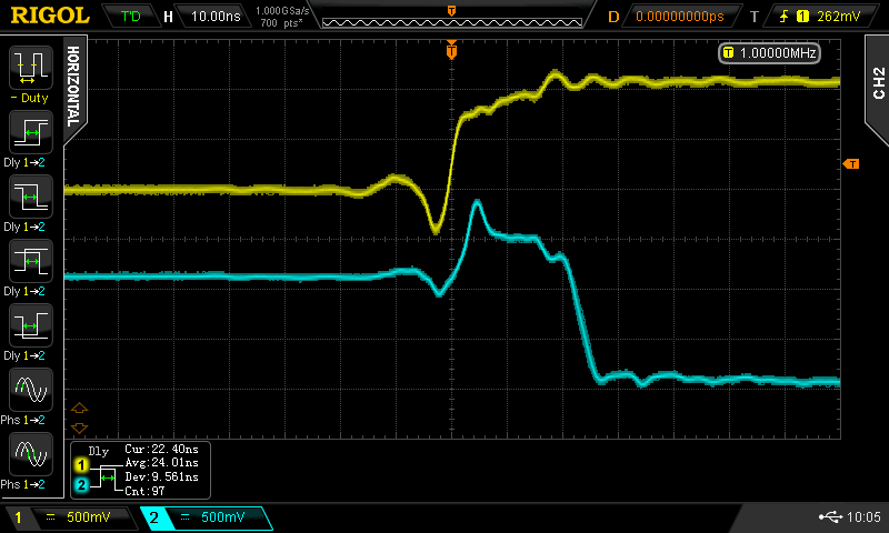
With the upper input driven the NAND shows a 3.0 ns TPLH and a 6.3 ns TPHL - the input speeds are now basically symmetrical unlike with the 1 nF speedup caps. This is good.
![]()
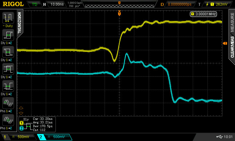
Oh, and if you drop the input frequency to 1 MHz or below, everything falls apart again. At DC, things work fine, as expected. I didn't measure the range of frequencies for which it's screwed up. I think this needs more bench time.
![]()
It's another mystery!
-
NAND Issues Resolved
01/15/2017 at 17:11 • 10 commentsYes, it was poor layout on the prototype. A long alligator lead used to pull one NAND input high had enough inductance to resonate with the input network and cause problems. I was able to simulate it in LTspice by adding an inductor where the long lead was. The yellow trace is the base of the upper NPN, and shows ringing like I saw on the hardware:
![]()
The 200 nH value was a complete guess - the actual inductance would depend on how I draped the alligator lead on the workbench, but the qualitative behavior was the same as I observed.
To fix the problem, I tied the upper input high with a very short wire. The circuit doesn't show the resonances anymore, but the propagation delay is still relatively long and somewhat sensitive to input pulse width. For instance, with a 1 MHz input signal, the propagation delay is around 16.5 ns, rising to 19.7 ns at 10 MHz:
![]()
![]()
On a longer timescale, the 10 MHz output still looks usable - I think you could go even higher:
![]()
Edge Rates
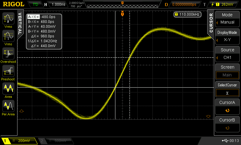
The fact that this circuit had issues with long leads on a "DC" input made me wonder about the edge speeds - that's what determines how much you have to worry about layout. The conservative rule of thumb is that you have to treat wires electrically longer than 1/6 of the transition time as transmission lines and terminate them at one or both ends to suppress waveform-distorting reflections. So, I decided to measure the edge rates.
In the book, "High Speed Digital Design: A Handbook of Black Magic", Johnson and Graham describe five methods for estimating the rise time of logic signals:
- Differentiating the step response to yield the impulse response then taking the standard deviation
- 10%-90% direct measurement
- 20%-80% direct measurement
- Center slope measurement
- Maximum slope measurement
(1) is interesting but too involved for now. (2) and (3) are complicated by the ringing, overshoot and odd shape of the waveforms. That leaves (4) and (5), which measure the slope of the rising edge, either at the center of the edge, or at the position of maximum slope. I just used cursors to measure the slope somewhere around the middle:
![]()
The measured slew rate is 440 mV / 960 ps = 0.458 V / ns. According to this site, this is about half the slew rate of 74HC logic at 5V supply, which is about 0.9V/ns. But, the supply here is 1.1V, only 22% as high as the 74HC. According to Johnson and Graham, this translates into a CBJT rise time of:
The same calculation for 74HC logic at 5V supply yields 5.5ns rise time, which agrees with 5ns figures I've seen quoted elsewhere. So, CBJT logic has edge rates about twice as fast as 74HC. While at first this might sound good, it means complications for laying out projects with CBJT logic. Light travels 72cm in 2.4ns, so you might have to treat wires as short as 12cm as transmission lines (assuming velocity factor = 1). You could add some more parts to slow the rise time (a simple RC network on the output would do it), but it detracts from the simplicity of the design. Maybe you can just add an extra RC at the output when you have a long run to drive.
-
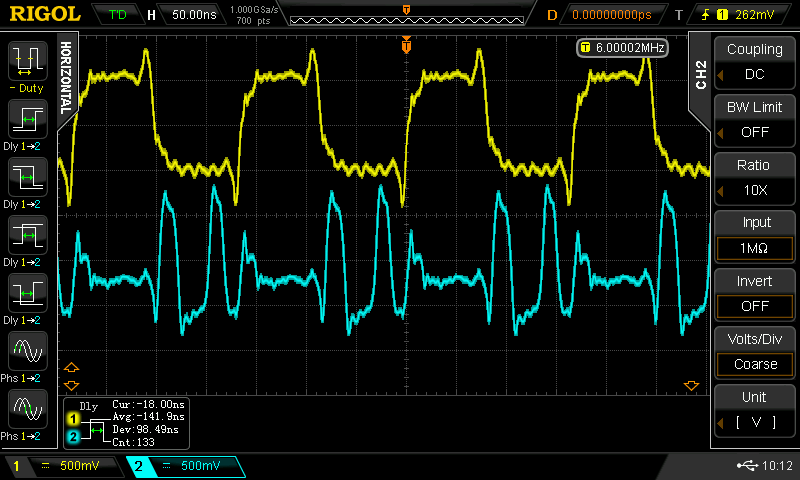
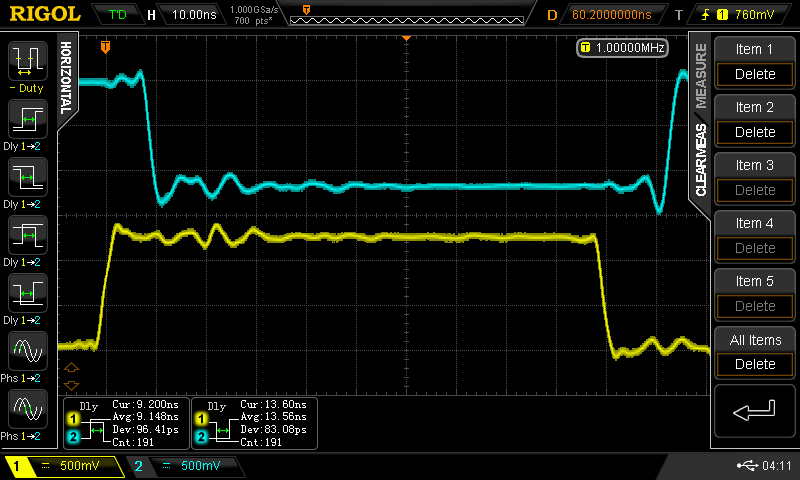
NAND hardware tests
01/15/2017 at 02:34 • 9 commentsUPDATE: the speeds measured here don't represent the true switching speed of these gates. See this log for more details.
I built a test jig for the simple NAND gate design. In order to drive it with "native" logic levels and impedances, I buffered the output of my signal generator (set to 1.1 V output amplitude) through a string of four inverters. This should produce close to a real CBJT drive for testing the NAND.
![]()
The gate design is as it was before: two 2N3904's in series on the low side, with two 2N3906's in parallel on the high side. I tested and simulated with a 1.1V supply.
![]()
At DC, the NAND gate works as expected. To test the high-speed performance, I drove one of the inputs while holding the other high. This turns the NAND into an inverter, and allows testing of the AC properties of the gate. Since the low-side transistors are in series, the two inputs are not identical - this caused the funny threshold seen in previous DC simulations.
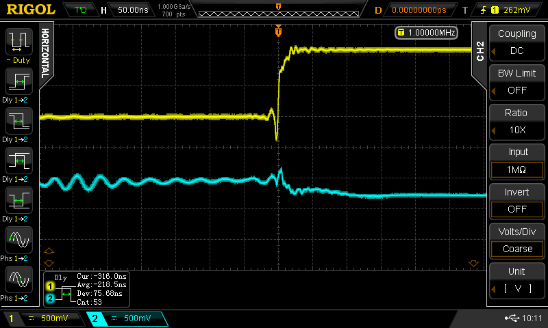
The upper input behaves roughly as expected with the lower input held high. Here's the waveform at the upper input (yellow) and the output (cyan) when driven at 1 MHz:
![]()
I measured the propagation delay as 9.5 ns for the H->L output transition and 4.7 ns for the L->H using cursors. The scope's auto-measurement came up with 7.48 ns and 4.5 ns for the same delays. Close enough - and not bad, really.
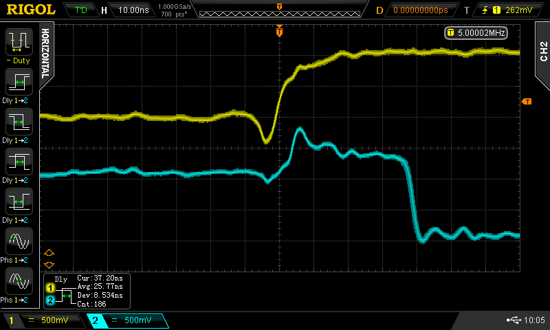
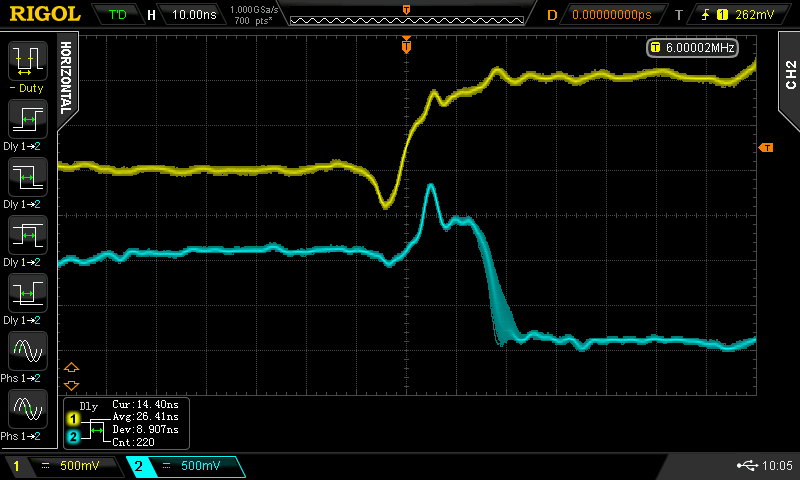
Testing the lower NAND input was much more interesting. There was a much bigger difference between the two propagation delays. Again, testing with a 1 MHz input signal, I measured 5 ns for the propagation delay when the output was going L->H - about the same as the upper input. But, the propagation delay for the other transition (H->L) was 20.7 ns, much longer than the upper input! Here's the L->H at ns delay:
![]()
vs the H-> at 20 ns:
![]()
I found this odd, partly because I hadn't seen any evidence of this in LTspice simulations. There, the delays are roughly identical:
![]()
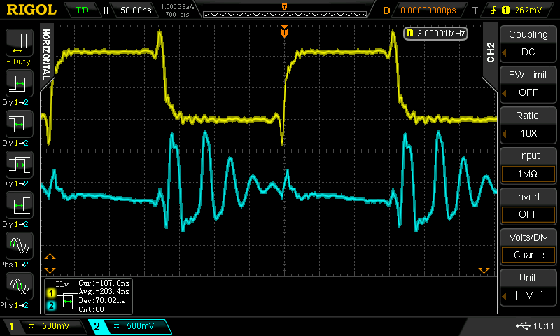
Two things come to mind: it could be bad spice models or parasitics in the layout. But playing around a bit found something even more odd - the delay depends on the input pulse frequency. At 1 MHz input, the delay was 20ns - this grew to a maximum of around 40ns with a 5 MHz input, but then the delay abruptly dropped again at 6 MHz! It was also clear that there was some instability involved - you can see in the the 6 MHz cyan trace (lower right). Here are 1, 3, 5, and 6 MHz plots. The output also peaks above the supply voltage before the transition ( you can also see this in the simulation above).
![]()
![]()
![]()
![]()
I probed around a bit, and found the problem (but not the solution) - there is some odd resonance on the node between the two 2N3904's. Here are the waveforms at that node (cyan) at the same frequencies:
![]()
![]()
![]()
![]()
You can see that the ringing starts when the input signal goes low. For long pulse widths, the ringing has died down by the next transition. For shorter widths, the ringing can interfere with the next edge, extending the delay time by an amount that depends on what phase of the ringing the edge coincides with.
I still don't know where that resonance is coming from. It doesn't happen in the simulation. I'll have to spend some more time with the board to figure it out. I think this can be fixed. Maybe it's just poor layout on the prototype.
Even if this is an unavoidable feature of these logic circuits, this behavior will just limit the maximum usable clock frequency.
Misc. Observations
It was a bit of a mystery how the output stage switches so quickly - shorter than the transistors should be able to turn off. I looked at the simulation closely - the transistors are still slow to turn off, but the opposing one turns on quickly and dominates the output. This causes some huge shoot-through current spikes in the output stage. It may be enough to warrant a bypass capacitor per output pair. This is just something you'd need to work around if you wanted to use this logic to build something.
The common LM317 "adjustable" regulator is a fixed 1.25V regulator in disguise. Just ground the adjustment pin and use it like a 78xx 3-terminal regulator and you get 1.25 V nominal output. One datasheet I read listed between 1.2 and 1.3 guaranteed, which might be a little much.
I've been thinking about a temperature-compensated regulator based on a couple of transistors as sensors and an LT3080 adjustable regulator. This would track the transistors Vbe and keep the supply in the sweet spot with variations in ambient. Of course, all the transistors would have to be at the same temperature for this to work - or close enough, anyway.
I don't have any immediate plans for this logic; other than trying to figure out this ringing business, I think I'm going to move on to other projects. But, I might design some boards for MMBT3904's and MMTB3906's in SOT23 packages because they're so small and cheap (as are 0603 R's and C's). Maybe a quad NAND or NOR gate and an edge-triggered flip flop. It would be interesting to wire up a counter and see how fast it will go.
-
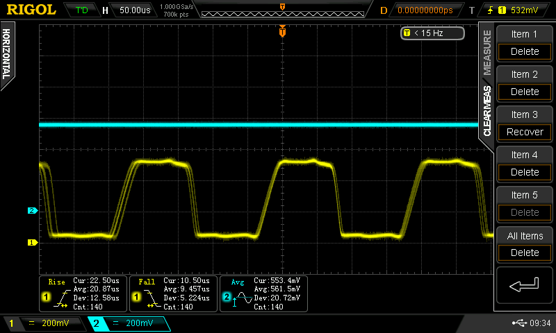
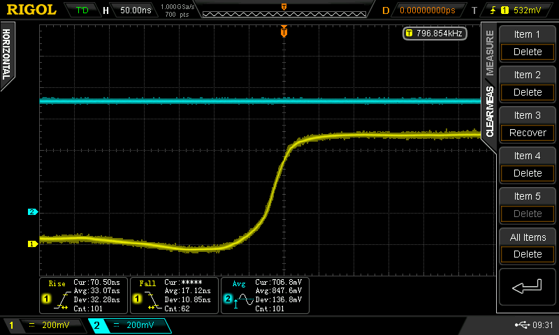
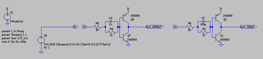
Speeding Up the NOT Gate
01/10/2017 at 02:04 • 22 commentsUPDATE: the speeds measured here don't represent the true switching speed of these gates. See this log for more details.
I played with the inverter simulation a bit - before testing the speed on the NAND gate, I figured I'd get things straight with the NOT. Adding the base resistors drops the power consumption as expected, but also dropped the oscillation frequency from 2.4 MHz to about 500 kHz. OK, I'll add the speedup caps. Simulations pointed to 1nF as a good value - which seemed large to me, but works OK on the board:
![]()
With the 1k base resistors and 1nF speedup caps added, I tested the ring oscillator at a bunch of different voltages. I hooked channel 2 (cyan trace) to the power lead to label the images with the supply voltage.
550 mV
Again, I saw oscillations down to about 0.4V supply voltage, but things only started to stabilize above 500 mV. Here it is running at about 5kHz.
![]()
707 mV
This logic is probably only truly usable above 700mV (at the temperature I tested at - whatever that was). The circuit runs at 796 kHz, implying a gate propagation delay of 12.5 us, with a rise-time of 70.5ns (fall time not captured).
![]()
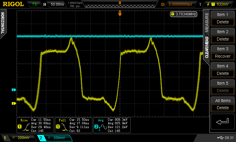
808 mV
By 808 mV, the speed has really picked up: f = 3.7 MHz, tpd = 27 ns, trise = 11.5 ns, tfall = 15.5ns. I forgot to measure the current.
Note that those peaks on the top and bottom are above V+ and below ground - I forgot to move channel 2's reference to match channel 1.
![]()
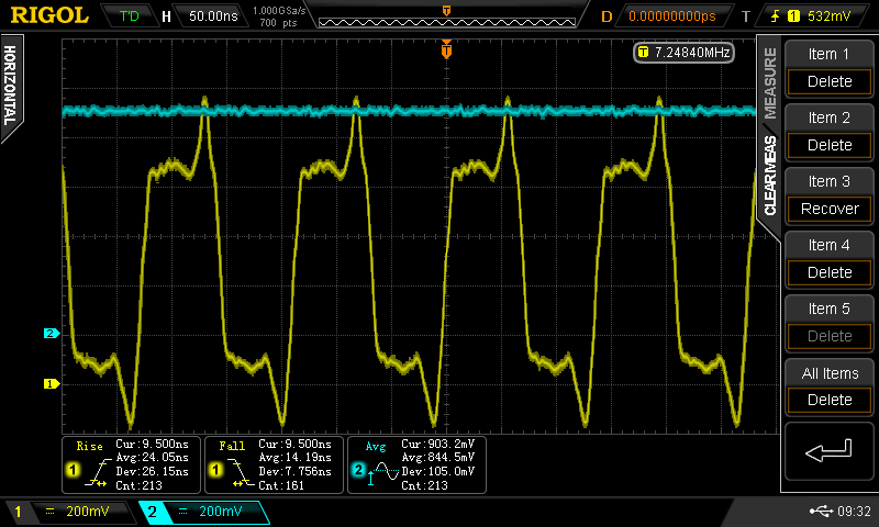
903 mV
The speed has doubled now. f = 7.2 MHz, tpd = 14 ns, trise = 9.5 ns, tfall = 9.5ns, current = 4 mA / gate
![]()
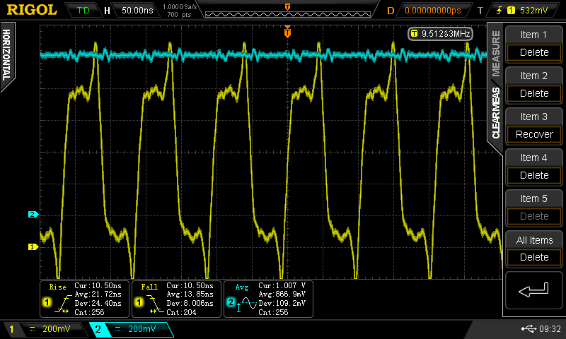
1.007 V
A more modest speed increase. f = 9.5 MHz, tpd = 10.5 ns, trise = 10.5 ns, tfall = 10.5 ns, current = 8 mA / gate.
I'm not sure I trust the scope's auto-measurement of rise and fall time with these waveforms. Next time I'm in the lab, I'll turn on the cursors and see exactly what it's measuring - although 1/5 of a division is 10 ns, which looks about right.
![]()
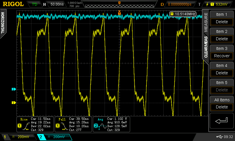
1.102 V
A little more speed. f = 10.51 MHz, tpd = 9.5 ns, trise and tfall about 10ns (scope auto-measurement screwed up), current = 12 mA / gate. This is probably the best voltage to run at.
![]()
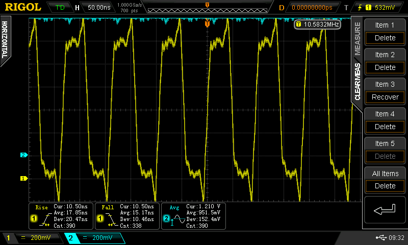
1.210 V
Not much speed increase, just consuming more power. f = 10.58 MHz, tpd = 9.5 ns, trise = 10.5ns, tfall = 10.5ns, current = 18 mA / gate.
![]()
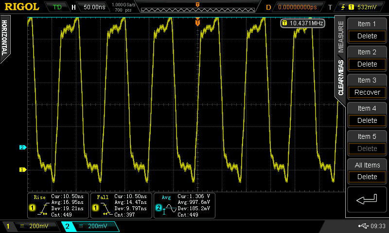
1.306 V
Speed reduced slightly, still more power consumption. 24 mA / gate now.
![]()
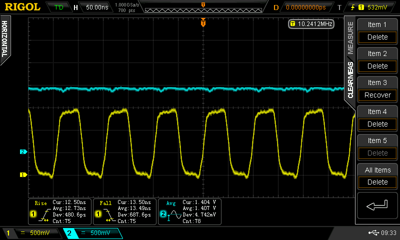
1.404 V
Less speed, more power - 30 mA / gate. The waveforms look superficially nicer, but at the cost of more than 3x the power used at 1.1V and a little less speed.
![]()
Summary
It looks like these inverters, with 1k base resistors and 1nF speedup caps, work best at around 1.1V supply. At this voltage, they show a propagation delay of about 9.5 ns. A look at the 74HC04 datasheet shows a typical 9ns tpd at 4.5V supply, which drops to 7ns at 5V supply. Amazingly, it would appear that this simple inverter is almost equivalent to 74HC logic in terms of speed. It doesn't seem like it should be...
When I get a chance, I'll wire a 5/6 of a 74HC04 into a similar ring, and see what that looks like.
-
CBJT NAND Gate
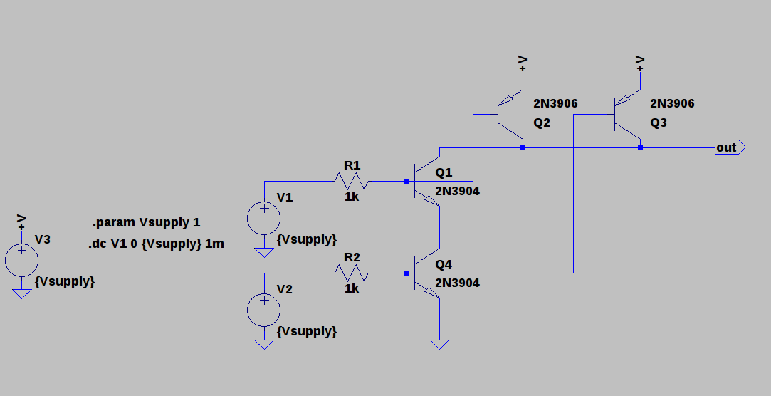
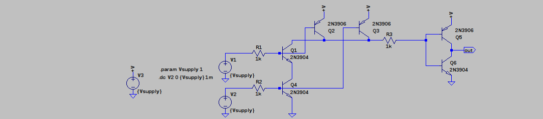
01/09/2017 at 01:17 • 11 commentsHere's a first try at a NAND gate. I took @Yann Guidon / YGDES's advice and went series on the bottom and parallel on top. If it works, the project is a success in some sense - every other gate can be constructed from NANDs. I've only simulated it so far.
![]()
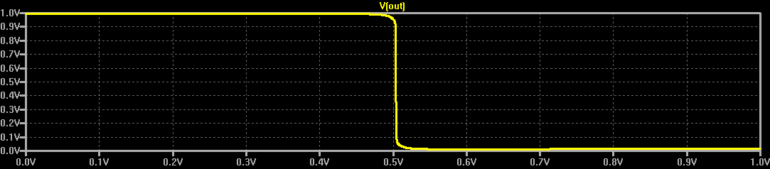
It's a straightforward adaptation of a simple CMOS NAND. I simulated the supply at both 0.8 and 1V, and it seems to work at either one, although a little better at 1V. The base resistors limit the input currents - these should have been on the inverter inputs, too. Because of the "stacked" input stage, the inputs are not symmetrical. For instance, here's the output voltage vs the top input with the bottom input held at logical 1 (1.0V):
![]()
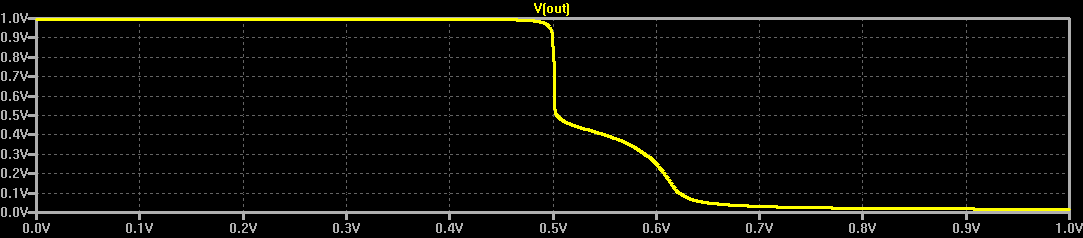
With the bottom input high, the NAND gate works like an inverter for the top input. And it looks like a pretty good one. The results aren't quite as good with the inputs reversed:
![]()
Here, with the top input held high, the threshold for the bottom input isn't great. Still, if you specify the Vih parameter (minimum high input voltage) as maybe 0.65V, then it should be fine.
I think this should be workable as a logic gate. I don't know about performance yet.
AND Gate
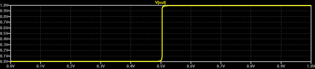
If you add another inverter stage to "clean up" the output, you get an AND gate with very nice thresholds on both inputs. Here's the circuit:
![]()
and the output with the top input high and the bottom swept (the "bad' curve above):
![]()
The output inverter produces nice thresholds for both inputs; their transfer functions are now basically identical.
CBJT Logic
Complementary bipolar junction transistor logic - like CMOS, but with NPNs and PNPs


 30%
30%
 40%
40%
 50%
50%
 60%
60%
 70%
70%
 80%
80%