 Tony Robinson
-
The Blinking Computer lives!
11/29/2021 at 11:19 • 0 commentsThe Blinking Computer never really died, it just ran at 0Hz for a while....
The original design had 5 general purpose registers and used a Raspberry Pi for RAM. It's sad but true that if your hardware skills are at my level everything has to be very very simple and the 128 bits of storage that the design called for along with some complex instruction sequencing was too much for me. So I really went down the rabbit hole of storage and simple architectures for a long time. Also I wrote a ton of code for the old architecture, including a Forth like language, floating point, random numbers, etc and that's now archived on github.
I hope I'm about to emerge from the rabbit hole. I have a CPU whose only state is the program counter and three flags (carry, zero and negative) which address 32 bytes of RAM. What's more it only has one sort of instruction, Mi = Mj OP Mk., that is load a couple of bytes, throw them through a simple (1 bit!) ALU and write the result back. I think this is as simple as it could ever be and still be useful as an educational computer (do leave feedback!). I've written some notes and even published a spreadsheet which runs simple code. -
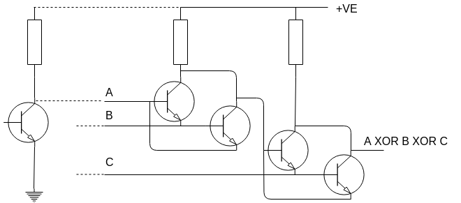
3 input XOR in 4T 2R
02/16/2019 at 10:50 • 10 commentsThis log is redundant - there is a complete Full Adder which uses this circuit at https://hackaday.io/project/160177-alu-in-dctl-technology/log/150451-full-adder and that work predates this and is more complete.
But, for the sake of not deleting valuable comments below, here it is (for now).
Addition can be decomposed into a carry chain (see past and future logs) and a three input exclusive OR operation which takes the two external inputs and the carry and produces the result.
https://hackaday.io/project/8449-hackaday-ttlers/log/150147-bipolar-xor-gate-with-only-2-transistors is the place to start for all things XOR. I'm just cascading two XOR in the same way as https://hackaday.io/project/160177-alu-in-dctl-technology/log/150451-full-adder and tweaking a few things.
![]()
The left hand side a typical BJT set up, some current sets a bipolar transistor to conduct or not, in which case either A is near ground or is wired to the +ve supply via a resistor. I've put it in to show that this is the input we need and also because it was what was needed to help me understand what is going on.
The output has the same characteristics as the left hand side, it's either to ground via a couple of BJT or to +VE via the resistor. I used 330 Ohm resistors, these being slightly faster than 10k. The BJTs are 2N3904s. Currently I'm getting just over 500 kHz, which is good enough.
-
Yet another memory cell - 2T
01/29/2019 at 09:25 • 8 commentsSo here I go again - here is another memory cell which I'd be pleased if the community could criticise.
For background, I want to build a discrete component CPU with enough LEDs so you can see how it all works and for it to be simple enough that others could build the design (e.g. for it to be a school 6th form project). It has quite a few registers, about 8, so that you can see how a processor works (smaller would be possible but tortuous to program). It's got a 16 bit instruction, data and address space to keep everything clean. So, just for the sake of keeping things clean there are a lot of memory cells to build, something like 16 x 8 = 128 and this could dominate the component count and so be the major blocker to other people building this processor.
So I want the smallest number of components to build a memory cell. The accepted smallest number is two, the standard DRAM design, in which a capacitor stores charge and is isolated by a MOSFET. Whilst I applaud the efforts to recreate these in discrete components (look at https://hackaday.io/project/8449-hackaday-ttlers/log/44217-dynamic-ram-with-single-mosfet-per-bit) I really can't get my head around the precharge and the sharing of the bit line between read and write. My CPU is meant as an introduction to everything from resistors through to compilers, so if it's not simple for me to understand then it's too complex for my processor.
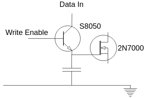
As a result I've done a lot of thinking and here is a 2 transistor memory cell using a capacitor to store the charge:
![]()
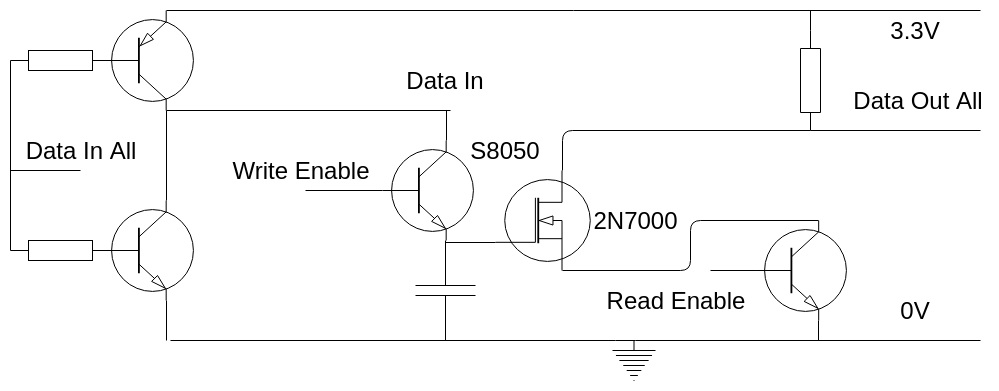
Or, showing all the shared components, here it is as part of a register file:
![]()
DataInAll is the data line for one bit position across all registers/words. It drives a NPN/PNP pair so that one conducts and the other doesn't. So DataIn is connected to ground or +ve. Provided WriteEnable is set low, then the capacitor keeps its charge, but if WriteEnable is set high then the capacitor will charge or discharge according to DataIn/DataInAll. Reading is done with the MOSFET, so it doesn't suck current from the capacitor. If ReadEnable is high then the state of DataOutAll is set by the state of the MOSFET, and the charge on the capacitor. Only one register/word has ReadEnable set high, so only one can pull down DataOutAll.
From playing about, it seems that the capacitor is not needed, I can use the gate capacitance of the MOSFET. So that's just two components for the memory cell. I can't get lower than two so hopefully I can now move on to fixing my diode ripple carry, the rest of the ALU, etc.
With no capacitor, things run fast. Using a RPi I can put data on DataInAll, assert write enable, wait, ground WriteEnable, assert ReadEnable, wait, read the data, ground ReadEnable all at 200kHz. That's as fast as I've got any of my memory cells to run, and is pushing the limits of WiringPi to set the GPIO (ultimately I'll abandon WiringPi).
Note that whilst I could use just the BJT and MOSFET (as above), the requirement that every state is visible means that I'm using the MOSFET to power a LED and running the read circuitry from that. I want two read lines, so I have the basic BJT and MOSFET as above (no capacitor) but then I'm using an LED two more BJT, one for each read line. So that's 5 components in total, not 2 as above, but a big improvement on the 21 components of my last written up memory cell.
-
DIY PCB - the problem of cheap visible circuit construction
03/08/2017 at 10:20 • 0 commentsThe biggest problem in this project has always been to create a processor that others can see what is going on, build it themselves and adapt it themselves.
This is quite a design challenge for me. I want all the components and wiring to be visible and I'd like the costs to come in at about £100 so that I don't put off others building and adapting. I believe this rules out standard PCBs.
I'm developing the idea or printing onto paper, sticking the paper on matrix board and mounting all components though the paper. All wiring is then visible on the front surface. I am allowing myself power supply wiring on the reverse, using map pins (or similar) on the visible side.
So far I like the idea. The white background gives good contrast and the finished circuit does look like the schematic, so making electronics visible, my main goal. Here is my first "PCB":
![]()
What I haven't got right yet is (a) what to print (b) I need whiter heavier paper (maybe plasticised) and (c) it's fiddly getting 4 legs down one hole. Oh, and it has to work of course, what you see above isn't soldered on the reverse, this is very much work in progress.
More detail at http://www.nanocpu.org/leds-and-wiring
-
A 2 transistor 9 diode memory cell
03/01/2017 at 15:53 • 0 commentsHere is (hopefully) the final memory cell architecture for my processor.
It uses two transistors as a flip-flop to store the state, S. There is also: IN - data in, WE - Write enable, OUT - data out and RE, Read enable.
Write is:
S = (S AND NOT WE) OR (WE AND IN)
(the NOT comes for almost free as it's shared across all 16 memory cells in a register).
Read is:
OUT = S AND RE
Both AND and OR may be implemented with two diodes and a resistor (e.g. http://electronics.stackexchange.com/questions/131860/diode-logic-gates). This is the simplest memory cell I can think of, if you double the write logic you can write to both halves of the flip-flop at the same time which improves speed - but I value simplicity over speed.
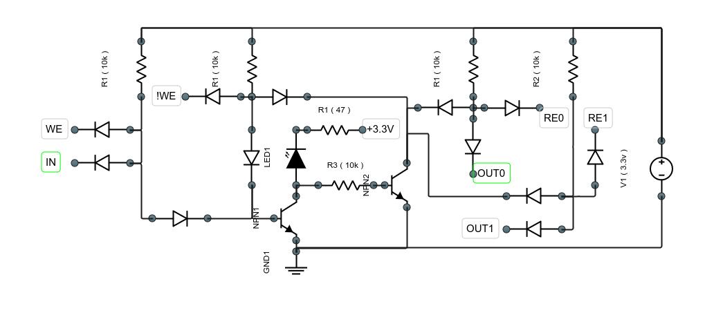
So, after fighting http://circuits-cloud.com/ all day (most saves fail and force a reload of the last successful save making progess painfully slow - I'm not using them again), here is the circuit diagram:
![]()
The left hand side does the write, the right hand side does the read (to two buses, 2T 9D is for only one read). Let's say we want to write, then we set WE high and the left AND circuit has the value of IN, where as the next AND circuit is low (as !WE is low). The OR of these two AND circuits is therefore the value of IN. Hence the base of NPN1 is set to IN, if it's high then the transistor conducts and the LED light is lit. R3 sends a low to NPN2 which is then off. When WE is low, !WE is high, so the output of NPN2 is fed back into NPN1 and a bit is stored.
The right hand side does the read and is considerably easier. Both OUT0 and OUT1 are AND functions of the relevant read enable signal (RE0 and RE1 respectively).
If anyone knows of a decent circuit layout for matrix board I really need it.
-
Fast carry propagation for a new ALU
02/23/2017 at 07:19 • 5 commentsI decided to redesign my ALU, the old one worked but it wasn't easy to see how it worked. It was too clever, I think people expect an ALU to compute everything (AND, OR, XOR, ADD/SUB, ASR) in a way they can see and then select the right output - that is much easier to understand.
Minimal ALUs are limited by the ripple-carry propagation time, so the first thing to do was to get my fast carry propagation design working. The slow bit of bipolar junction transistors is switching them off, so I got rid of all of them and used diodes to do all the carry propagation (these will be Schottky diodes for fast switching and low voltage drop). So here it is in it;s simplest form:
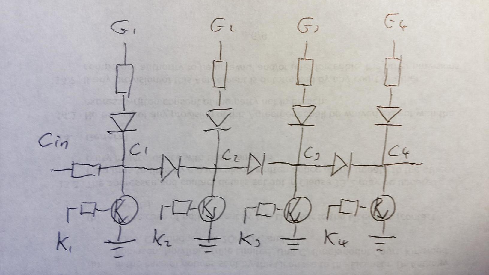
![]() Generate, G, is high if both inputs are high. Kill, K, is high if both inputs are low. The carry goes in on the left, if K1 is high then the first NPN is on and the carry is grounded, if G1 is high then the carry out is high else the carry is propagated. That's pretty simple, I feel confident I can both get this implemented in a way that you can see the signal flow (as above) and thus be able to explain how this time-critical bit of a CPU works to all.
Generate, G, is high if both inputs are high. Kill, K, is high if both inputs are low. The carry goes in on the left, if K1 is high then the first NPN is on and the carry is grounded, if G1 is high then the carry out is high else the carry is propagated. That's pretty simple, I feel confident I can both get this implemented in a way that you can see the signal flow (as above) and thus be able to explain how this time-critical bit of a CPU works to all.There's more detail at http://www.nanocpu.org/alu
-
the state machine - or lack of one
02/09/2017 at 20:40 • 0 commentsWow, the state machine of the CPU is hard - really hard. I thought I should start with what took the most real estate, the ALU and the memory cells, now I think I'm (touch wood) on top of both of those (I will update logs with progress as and when) but I'm struggling with the state machine - that is the bit of logic that raises all of the right enable lines at the right time. I shouldn't be at all surprised, there's a few people on home-built computers web-ring who said the same thing - it's the go-to site.
So this isn't really a log entry as I don't have a state machine. What I find fascinating is that a CPU is something that, in my software world, runs compiled code (leaving aside the fact I run Python under Linux in a VM running Windows) but is really something that may execute microcode which may execute itself to fetch instructions (my I = *P++) which executes a state machine which executes a set of control lines which executes a set of logical functions which are expressed as analog signal processing where semiconductor physics (my almost-lost first degree) does the hard work.
So many levels. I really don't like public speaking unless I have something worthwhile to say, but taking all this from a "BASIC" language through FORTH, assembly code, right the way down to the electrons and holes is something I feel confident I can engage and audience with. Teaching technology is not my goal - my goal is to encourage others to explore their dreams, however corny that sounds. But to do that I've got to succeed and that's a lot more time and effort away that I can plan for (even when you take into account Hofstadter's law).
-
3.3v vs 5v
01/27/2017 at 19:17 • 14 commentsRight now my #1 question to sort out is should I run this at 3.3v or 5v? 3.3v has the advantage that transistors switch faster, and I'm an optimiser so I would like this. However I love blue LEDs and have just bought a thousand of them, these are on max current when wired 3.3v -> LED -> NPN -> ground without a current limiting resistor. Should I worry that the LED might short and so blow the lot? (yes I think so). Also my new carry logic uses a diodes ladder which would like 5v much more than 3.3v (at a pinch I could use 5v just for this). So what should it be, 3.3v or 5v - I have yet to decide.
[ I've been out of the country on a work trip so haven't had any time for this in the last week and a bit - some new Schottky diodes have arrived and I need to stress test my new memory cell - time to take a day's holiday I think ]
P.S. it seems that there is a maximum thread depth which is stopping me replying directly below some of the comments. As a result they are appearing above which does confuse the flow.
The Blinking Computer
An educational 16-bit CPU made from < 1024 transistors with lots of LEDs that anyone can build and learn from

 Generate, G, is high if both inputs are high. Kill, K, is high if both inputs are low. The carry goes in on the left, if K1 is high then the first NPN is on and the carry is grounded, if G1 is high then the carry out is high else the carry is propagated. That's pretty simple, I feel confident I can both get this implemented in a way that you can see the signal flow (as above) and thus be able to explain how this time-critical bit of a CPU works to all.