Johnny
-
Test Code
01/16/2018 at 03:58 • 1 comment/* * Test File for Modular IN12A Nixie Display Boards * Works with Arduino Uno. * * By: Johnny Izzard */ #include <SPI.h> #define LD 10 #define CLK 13 #define SDO 11 #define PWM 9 #define tube_off 10 #define ind_off 3 uint16_t decimal_lookup[11] = {0x0001, 0x0002, 0x0004, 0x0008, 0x0010, 0x0020, 0x0040, 0x0080, 0x0100, 0x0200, 0x0000}; // decimal_lookup[0]...decimal_lookup[9] outputs corresponding nixie number. decimal_lookup[10] is off. uint8_t ind_lookup[4] = {0x01, 0x02, 0x03, 0x00}; // ind_lookup[0] is top indicator, ind_lookup[1] is bottom indicator, ind_lookup[2] is both, ind_lookup[3] is off. uint32_t data1 = 0; // Used to store data to be shifted uint32_t data2 = 0; uint32_t data3 = 0; uint8_t tube1 = 0; // Value to display on the corresponding tube. uint8_t tube2 = 0; uint8_t tube3 = 0; uint8_t tube4 = 0; uint8_t tube5 = 0; uint8_t tube6 = 0; uint8_t indicator1 = 0; // Value to display on the corresponding indicator. uint8_t indicator2 = 0; uint8_t indicator3 = 0; void setup() { pinMode(LD,OUTPUT); // LD is pin 10 (active high) pinMode(CLK,OUTPUT); // CLK is pin 13 pinMode(SDO,OUTPUT); // SDO is pin 11 pinMode(PWM,OUTPUT); // PWM (Blank) is pin 9 (active low) digitalWrite(LD,LOW); digitalWrite(CLK,LOW); digitalWrite(SDO,LOW); digitalWrite(PWM,HIGH); SPI.beginTransaction(SPISettings(1000000, MSBFIRST, SPI_MODE1)); /* Reset Values/Blank The Display */ tube1 = tube_off; tube2 = tube_off; tube3 = tube_off; tube4 = tube_off; tube5 = tube_off; tube6 = tube_off; indicator1 = ind_off; indicator2 = ind_off; indicator3 = ind_off; update_disp(); } void loop() { indicator1 = 2; // Both indicators on indicator2 = 2; indicator3 = ind_off; for(uint8_t i = 0; i<10; i++){ tube1 = i; tube2 = i; tube3 = i; tube4 = i; tube5 = i; tube6 = i; update_disp(); delay(500); } /* Reset Values/Blank The Display */ tube1 = tube_off; tube2 = tube_off; tube3 = tube_off; tube4 = tube_off; tube5 = tube_off; tube6 = tube_off; indicator1 = ind_off; indicator2 = ind_off; indicator3 = ind_off; update_disp(); delay(500); tube1 = 9; update_disp(); delay(500); tube1 = tube_off; tube2 = 9; update_disp(); delay(500); tube2 = tube_off; indicator1 = 0; update_disp(); delay(500); indicator1 = 1; update_disp(); delay(500); indicator1 = 2; update_disp(); delay(500); indicator1 = ind_off; tube3 = 9; update_disp(); delay(500); tube3 = tube_off; tube4 = 9; update_disp(); delay(500); tube4 = tube_off; indicator2 = 0; update_disp(); delay(500); indicator2 = 1; update_disp(); delay(500); indicator2 = 2; update_disp(); delay(500); indicator2 = ind_off; tube5 = 9; update_disp(); delay(500); tube5 = tube_off; tube6 = 9; update_disp(); delay(500); tube6 = tube_off; indicator3 = 0; update_disp(); delay(500); indicator3 = 1; update_disp(); delay(500); indicator3 = 2; update_disp(); delay(500); indicator3 = ind_off; update_disp(); delay(500); // All On tube1 = 9; tube2 = 9; tube3 = 9; tube4 = 9; tube5 = 9; tube6 = 9; indicator1 = 2; indicator2 = 2; indicator3 = 2; update_disp(); // Fade Out for(uint8_t i = 150; i!=0; i-=1){ analogWrite(PWM,i); delay(40); } // Fade In for(uint8_t i = 0; i!=150; i+=1){ analogWrite(PWM,i); delay(40); } digitalWrite(PWM,HIGH); } void update_disp(void){ data1 = 0x00000000; data1 |= ((uint32_t (decimal_lookup[tube1]))&0x000003FF); data1 |= ((uint32_t (decimal_lookup[tube2])<<10)&0x000FFC00); data1 |= ((uint32_t (ind_lookup[indicator1])<<20)&0x00300000); data2 = 0x00000000; data2 |= ((uint32_t (decimal_lookup[tube3]))&0x000003FF); data2 |= ((uint32_t (decimal_lookup[tube4])<<10)&0x000FFC00); data2 |= ((uint32_t (ind_lookup[indicator2])<<20)&0x00300000); data3 = 0x00000000; data3 |= ((uint32_t (decimal_lookup[tube5]))&0x000003FF); data3 |= ((uint32_t (decimal_lookup[tube6])<<10)&0x000FFC00); data3 |= ((uint32_t (ind_lookup[indicator3])<<20)&0x00300000); digitalWrite(LD,HIGH); SPI.transfer(data1>>24); SPI.transfer(data1>>16); SPI.transfer(data1>>8); SPI.transfer(data1); digitalWrite(LD,LOW); digitalWrite(LD,HIGH); digitalWrite(LD,HIGH); SPI.transfer(data2>>24); SPI.transfer(data2>>16); SPI.transfer(data2>>8); SPI.transfer(data2); digitalWrite(LD,LOW); digitalWrite(LD,HIGH); digitalWrite(LD,HIGH); SPI.transfer(data3>>24); SPI.transfer(data3>>16); SPI.transfer(data3>>8); SPI.transfer(data3); digitalWrite(LD,LOW); digitalWrite(LD,HIGH); } -
INS-1
12/17/2015 at 08:05 • 3 comments![]()
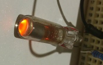
I'm trying out the INS-1 indicator bulbs to replace the generic ones I use.
Datasheets are still in Russian, but google translate to the rescue!
![]()
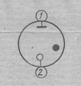
Designator Electrode Type 1 - The smaller cylinder Anode 2 - The larger cylinder Cathode See the dark dot in the pinout diagram? This matches a dot on the envelope of the indicator (image below). The dot is next to the anode pin. Another way of tell the anode from the cathode, as the table above suggests, is finding the pin that connects to the smaller cylinder.
![]()
Parameter Name Minimum Maximum Firing Voltage, in V 65 90 Sustaining Voltage, in V - 55 Recommended current, providing sufficient brightness is 0.5mA.
Because the sustain voltage is about 55V, I'm using a 180V power supply and 0.5mA is required, about 270K current limiting resistor is used.
-
6 Digits + Brightness
12/01/2015 at 06:22 • 0 comments -
4 Digits
11/27/2015 at 11:20 • 0 comments -
Module Test
11/27/2015 at 09:30 • 0 comments -
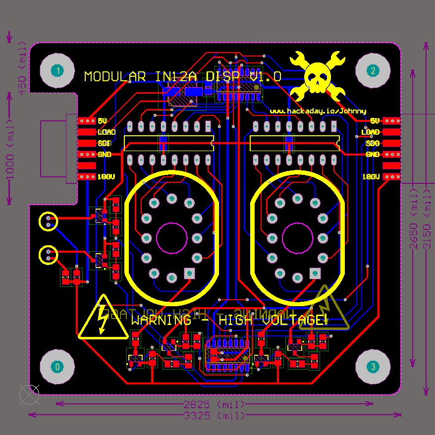
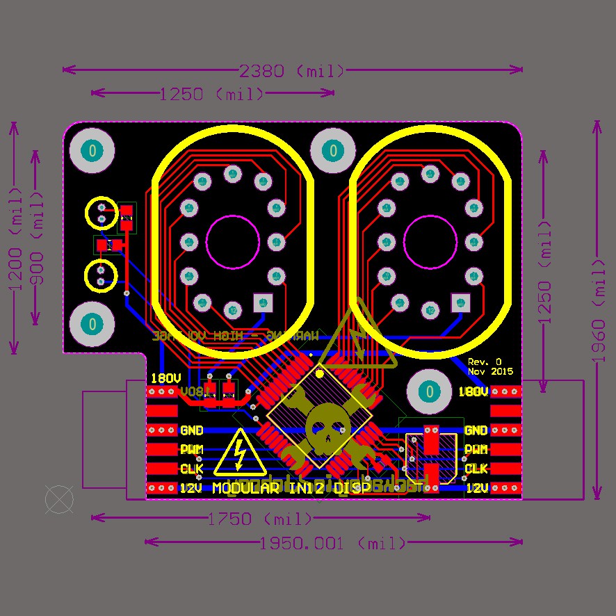
PCBs
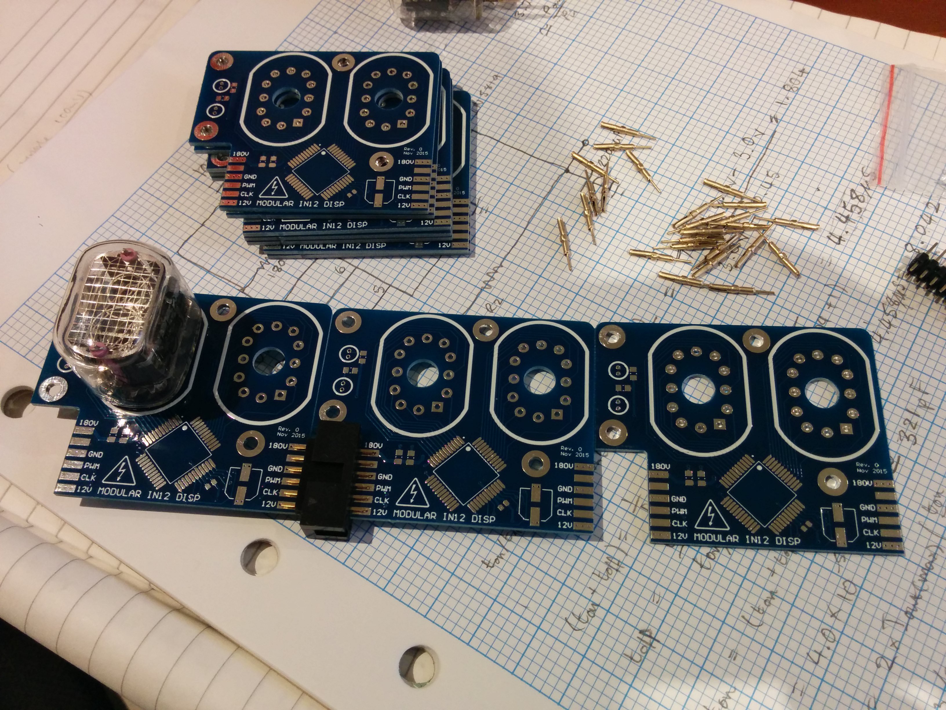
11/27/2015 at 07:13 • 0 commentsPCBs arrived. I populated one and gave it a test program. All works well.
![]()
![]()
-
Better Driving Solution
11/05/2015 at 03:06 • 0 commentsCame across this component the other day:
![]()
![]()
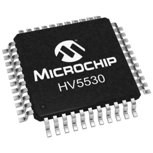
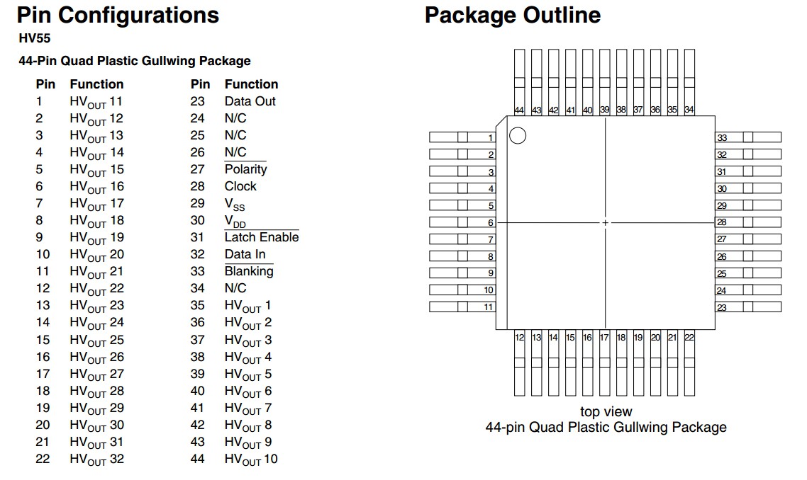
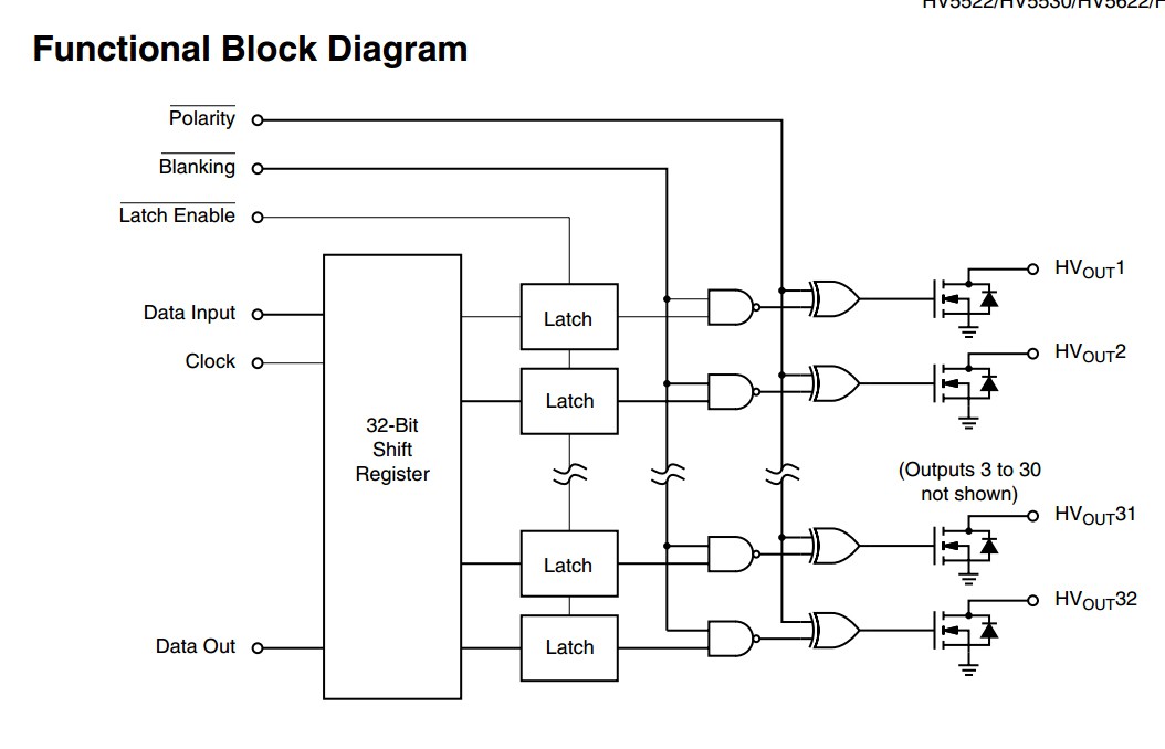
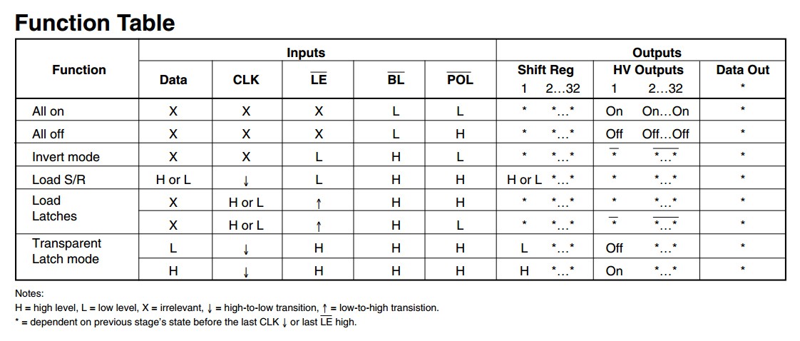
It's a 32-bit serial-in parallel-out shift-register with open drain outputs designed for driving high voltage loads, perfect for nixie tubes. The shift-register has typical 'Data In', 'Clock' and 'Data Out' pins. The active-low 'Latch Enable' pin is used to latch/save the data stored in the shift register to the buffer/output register, which in turn, turns on the appropriate output MOSFET. The 'LE' pin should be kept at logic-high in rest state, then send a logic-low pulse to latch. The active-low 'Polarity' pin can be used to invert the outputs on logic-low and the active-low 'Blanking' pin will turn off the outputs on logic-low (this doesn't change the buffer value and note the polarity function has higher priority). The 'BL' pin can be used to change the displays brightness using PWM. The HV5530 shifts data anticlockwise around the IC, where it's brother, the HV5630 shifts clockwise. This is useful for different PCB layouts. But in truth you could just change to shifting order from MSB to LSB or vice-versa in your program. If you plan on using SPI with the HV5530, note that MODE1 or MODE2 should be used with MSB first. MODE1 or MODE2 are used because the HV5530 and HV5630's shift-register latches data on the falling edge of the 'CLK' pin.
![]()
![]()
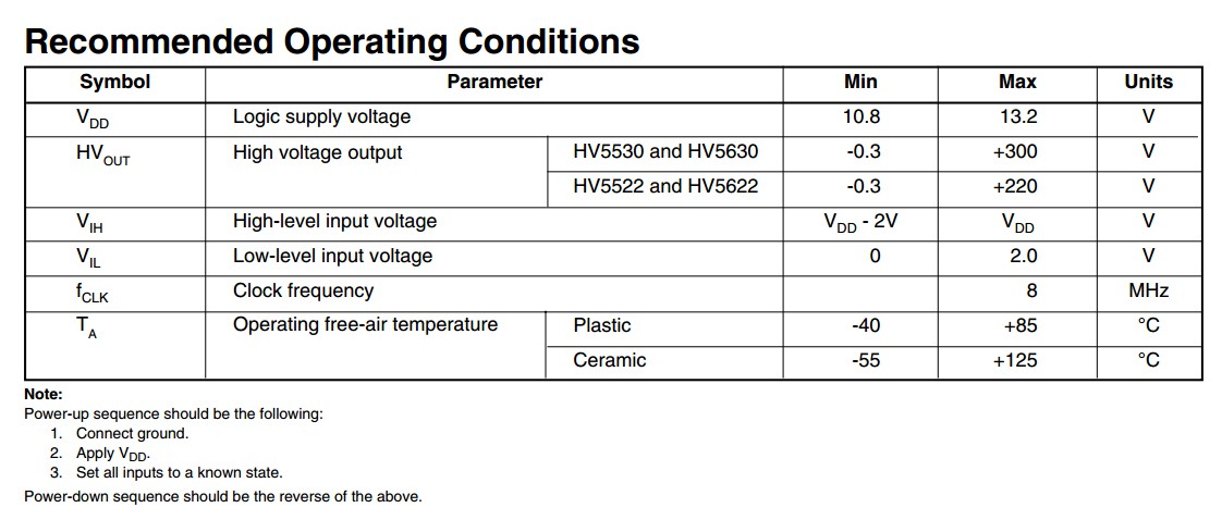
The voltage requirements for this device are a bit of a downer, as it's not 5V CMOS compatible (technically). 12V logic is specified by the datasheet, but in practice I've used 5V logic fine. In my case 12V is needed for my SMPS to produce 180V for the nixies; so the 12V here can be used in conjunction with a level shifting circuit to convert 5V signals to 12V signals.
![]()
The real positives for this device are:
- It's still being manufactured, unlike the SN74141 and K155ID1.
- Replaces many components and number of tracks, resulting in a much more compact board.
Cons:
- 12V CMOS logic
- Costly at about $6USD each
My original driving solution using the K155ID1 with 73HC595 resulted in a design that looked like this:
![]()
The new design using the HV5530 looks like this:
![]()
-
Driving the IN-12A
11/15/2014 at 12:46 • 0 comments![]()
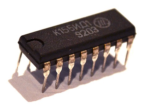
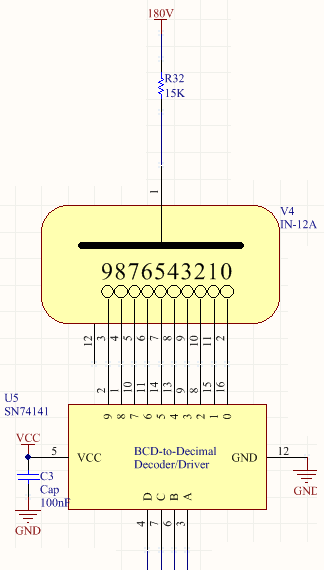
The IN-12A nixie tubes are operated at very high voltages, and microcontrollers can't handle voltages much higher then their VCC voltage. So that the IN-12A's can be controlled by digital logic circuitry, it is required that we have some sort of device that can drive these nixies, but also be able to interface with a microcontroller. The easiest method is a driver that can pull individual cathodes (numbers) to ground. Traditionally a SN74141 BCD(binary coded decimal)-TO-DECIMAL driver/decoder is used. This part is very rare these days, and if you do find one on ebay, it most likely will be second hand, and will cost you an arm and a leg.
An alternative to the SN74141 is the K155ID1, a SN74141 clone made in Russia in the late 80s. The K155ID1 is not as expensive as the SN74141 but, is still quite expensive, at about $2US a piece when purchased in lots of 6 and above. With that in mind, that's about $12US for six nixie drivers when making a six digit clock. As the K155ID1 stopped being manufactured long ago, and the NOS (new old stock) will eventually run dry, prices will go even higher. Because of this I will show an alternative options in a later project log.
![]()
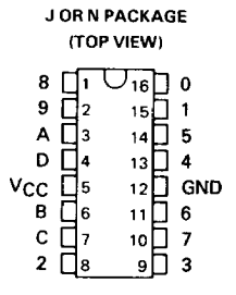
The K155ID1 is a BCD-TO-DECIMAL driver/decoder. How this works is, when a binary value is placed on the A-D (A is the least significant bit or bit 0) input pins, a corresponding output pin with the decimal value name will go LOW. That means that the K155ID1 has ACTIVE LOW outputs. The output pins of the K155ID1 are open collector, so they can pull to ground (LOW), but cannot produce a logic HIGH output. Instead, when a output pin is not LOW, the output is high impedance. Open collector TTL ICs like these are designed to drive loads, not for digital communication.
![]()
A useful feature of the K155ID1 is, when the binary input goes higher than the decimal range (9), all the outputs become high impedance. This is useful for blanking (turning off) the nixie tube.
-
The IN-12A
11/13/2014 at 07:58 • 0 comments![]()
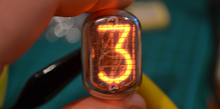
The IN-12A is a relatively cheap 80s cold cathode tube made is Soviet Russia and is by far the most common nixie found on ebay. Price is around $20US for a lot of six (new old stock).
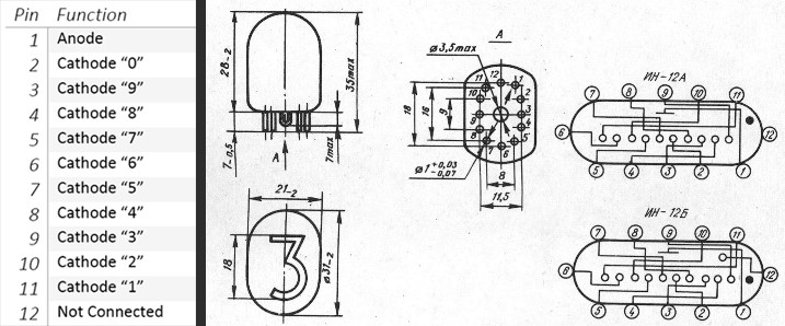
The IN-12A has 12 pins. Pin 1 is the anode. This pin is tied to 170-200V DC. Pins 2-11 are the individual number cathode pins. When you want to illuminate a particular number, place 0V on the corresponding cathode pin (be sure to include a current limiting resistor on the anode pin, seen further in the log). Please refer to the image and table below.
![]()
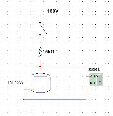
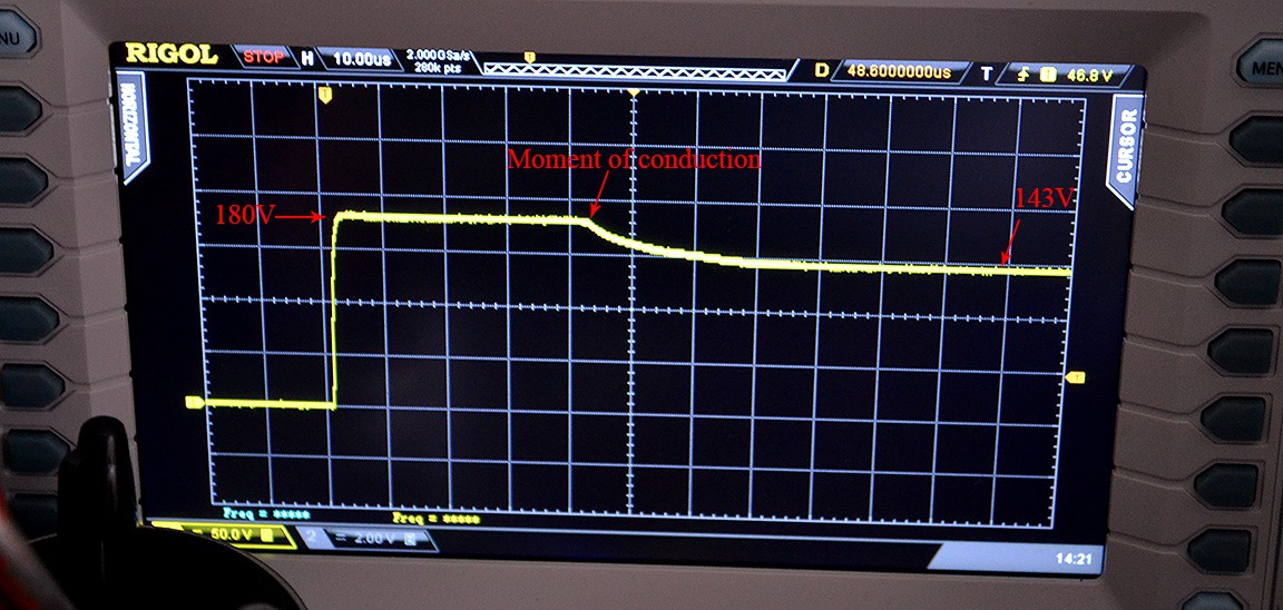
The IN-12A has a strike voltage of about 170V, that is the voltage at which conduction between the anode and cathode can begin so the number can illuminate. For conduction to start, it takes time, as the nixie's gas needs an ionized path from anode to cathode. Once conducting, the anode to cathode voltage will drop and current will increase. Both will reach a steady state in about 100us.
![]()
Like the test circuit seen above, 180V from a boost converter was applied to the nixie tube's anode through a series 15K current limiting resistor and GND was applied to the number three cathode. After conduction, the anode to cathode voltage dropped to about 143V. This is below the strike voltage now, but don't worry, the ionized gas path will remain, this is normal... The current through the nixie tube ended up at about 2.5mA, which is the nominal value for the IN-12A.
![Anode to Cathode Voltage at Switch Closed O-Scope Reading]()
The oscilloscope trace above is an example of testing a cathodes step response (number three cathode). The trace may vary slightly for different number cathodes, as the anode to cathode distance and cathode surface area varies. Analyzing the oscilloscope trace, it can been seen that it takes about 80us for the number three cathode to reach steady-state. A comparison between cathode settling times needs to be taken into consideration if I wish to use PWM to effect the brightness of the display.
![]()
-
PrototypeVideo
07/17/2014 at 07:37 • 0 commentsThis is the proof of concept board. This will be re-designed for fab-house manufacturing. Two layer, and much smaller.
Modular Nixie Display
Modular nixie display board based on the soviet Russian IN-12A cold-cathode tubes.