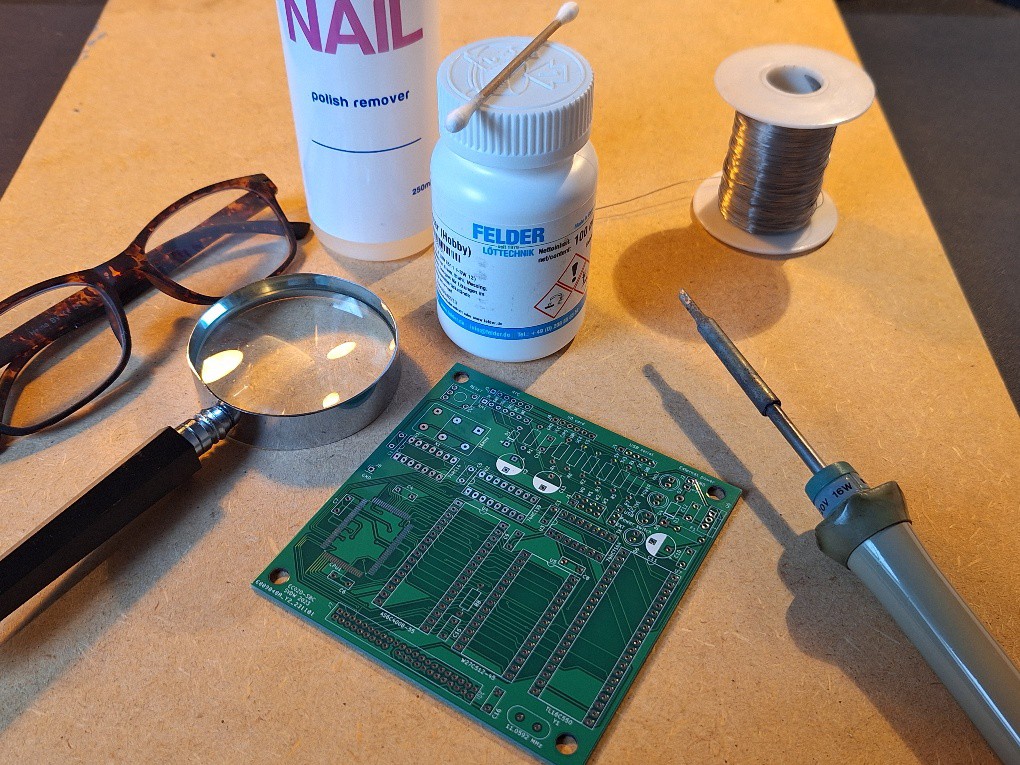
First, obtain all the components. Both the CPU (MC68EC020FG25) and the EEPROM (W27C512) can be ordered from suppliers in China. When searching for the CPU, use its full name to locate it in the store.
The other components can be ordered from your preferred supplier.
Order the PCB; since it's only 10x10cm, it can be produced very cheaply.
The total cost will be between €50 and €100.
2
Soldering the CPU
Start by soldering the CPU; it can be done with a regular soldering iron. Refer to the internet for guidance on soldering this SMD component (SMD soldering tutorial). The trick is to use flux (and very little tin). For me, this was the first time I soldered an SMD, and it was successful.
Check for loose connections by using a small screwdriver to inspect each contact.
Check visually for short circuits using a loupe, microscope, and/or your grandfather's glasses (+3).
Check for short circuits by using a multimeter and test A0 with A1, A1 with A2 etc. This can be done easily within the RAM-socket. Check also D24 and D25, etc.
3
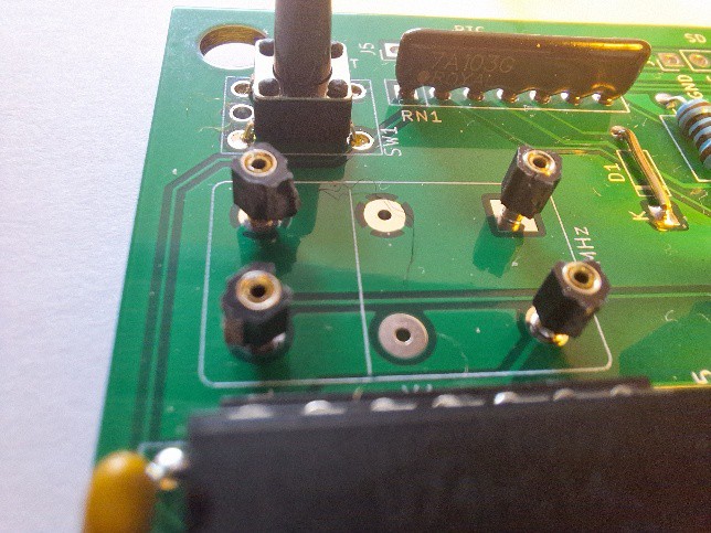
Solder the first components
Create a custom socket for the X-tal oscillator from some female pinheads.
Solder the 74HC14.
Solder the optional power supply.
Solder the power LED/resistor.
Solder the power switch / header.
Solder the decoupling capacitors (100 nF) around the chips.
Solder the resistor array.
4
Free run (optional)
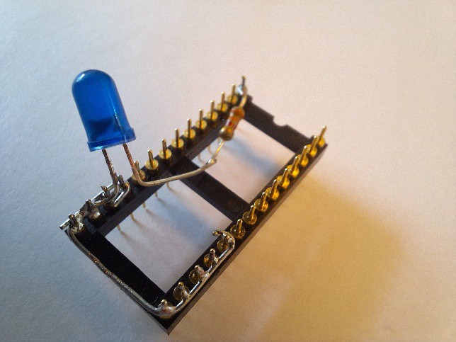
Although optional, it is highly recommended to test the board so far with the free run test. Connecting the databus to the ground, the CPU will read in 0x0000.0000 as an instruction and will execute a kind of NOP (in fact, it will execute ORI.b #0,D0). It will proceed to the next address, covering the entire address space (0xFFFF.FFFE). Then it will return to address zero again.
By creating a small tool (see picture), it is possible to test the CPU and base connections. A LED connected to the highest address line will blink rapidly. (I built this on the EEPROM socket, but perhaps it's better to use the RAM socket. There are more address lines, so the LED will blink slower).
Build the free run tool (D0-D7 connected to the ground).
Place the 74HCT14.
Place a 8 MHz oscillator.
Use a multimeter to measure the current, it should be about 150 ~ 200 mA.
If the current is higher, disconnect the power immediately and search for short circuit.
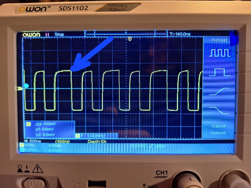
Use an oscilloscope to check all the address lines; they should exhibit a perfect square wave (A1 to A23). The address lines can be accessed through the RAM socket.
Due to the internal instruction cache, A0 will follow a zero-one-zero-one pattern. The 68020/68030 always reads in longwords/32 bits into the instruction cache. After the 32 bits instruction fetch (in fact, two 16-bit instructions are read into the cache), the two instructions will execute. A0 will remain high for two additional clock ticks (see the picture below).
In more detail, this CPU operates at 8 MHz, and the oscilloscope measures an average frequency of 1.143 MHz. So, 8/1.143 results in an average of 7 clock ticks per square wave. For a 32-bit instruction fetch, A0 continues in a zero-one-zero-one pattern, representing two square waves, consuming a total of 2*7=14 ticks. Reading one byte from RAM takes 3 cycles, so reading a 32-bit longword on a 8 bits wide bus takes 4*3=12 cycles. That leaves 2 ticks for executing the two ORI instructions.
Without the free-run-tool it would be hard to get this image on a simple scope.
5
Completing the build
If the free-run test passed, proceed with the remaining components
Solder sockets for the EEPROM/RAM and other chips.
Solder the passive components.
Solder the headers and reset button.
Check the 100 Hz oscillator; if the deviation is too large, replace the capacitor with another one.
6
BIOS
I'll attach a simple BIOS; it mainly initializes the hardware and is capable of receiving an S-file. Most traps are Easy68K compatible. Of course, you can use your own BIOS!
Program the EEPROM with a BIOS (with a TL866ii plus)
Discussions
Become a Hackaday.io Member
Create an account to leave a comment. Already have an account? Log In.