 Capt. Flatus O'Flaherty ☠
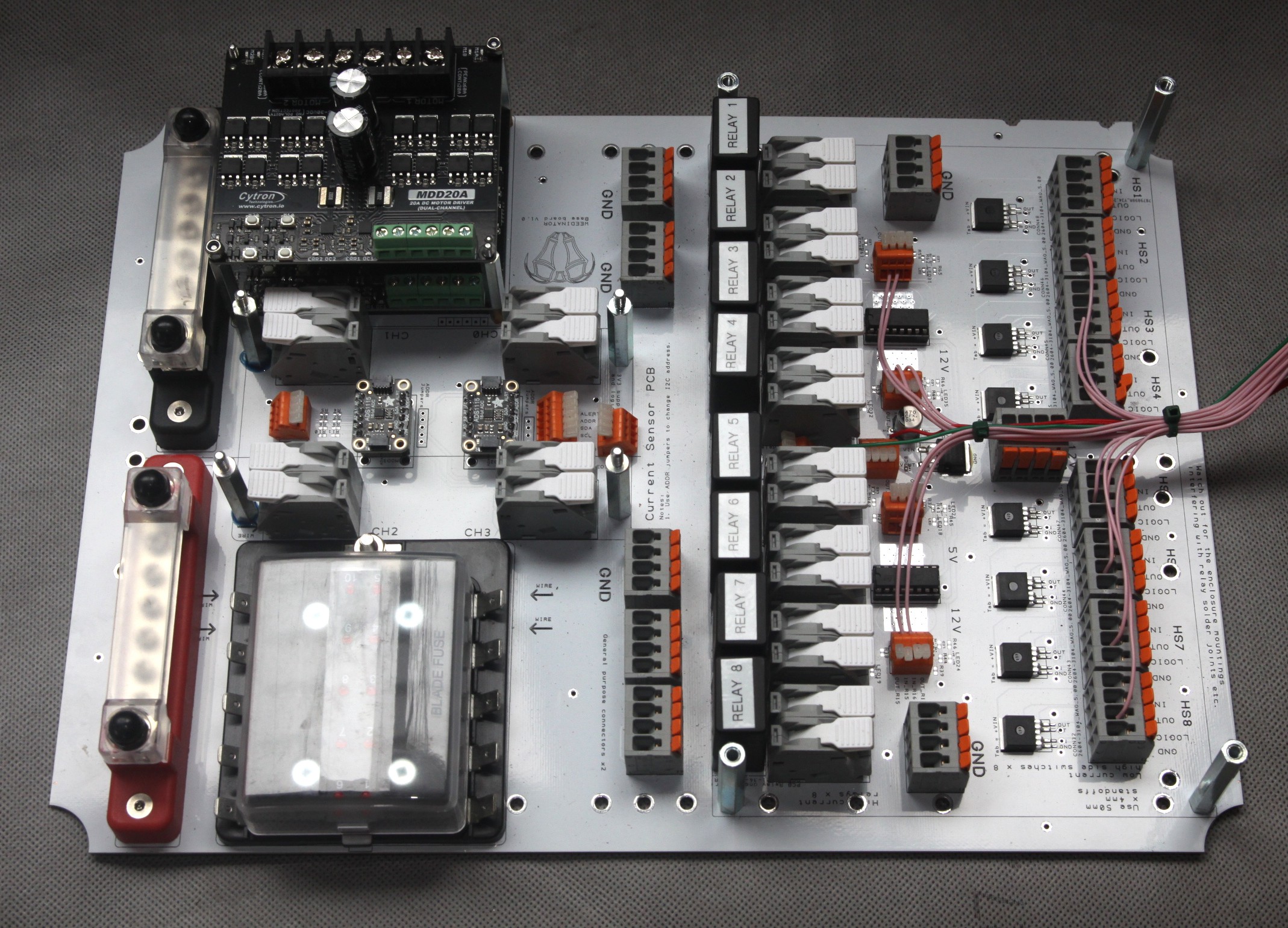
Large PCBs are expensive, but in this situation it seems to be appropriate to use one to fill the lowest layer of the control box. The new base PCB has a bank of High side switches, relays and a current sensing module are included. Other components such as bus bars, motor drivers modules and fuse box are bolted on. Layers of PCBs can be built up upon the base board such as extra motor drivers, current sensor modules, a large bank of high side switches and/or a large bank of relays.
The underside of the board has captive four pronged nuts for the bus bars and heavy, solid 2mm copper lugs for connecting the 40 amp relays to their grey Wago connectors.
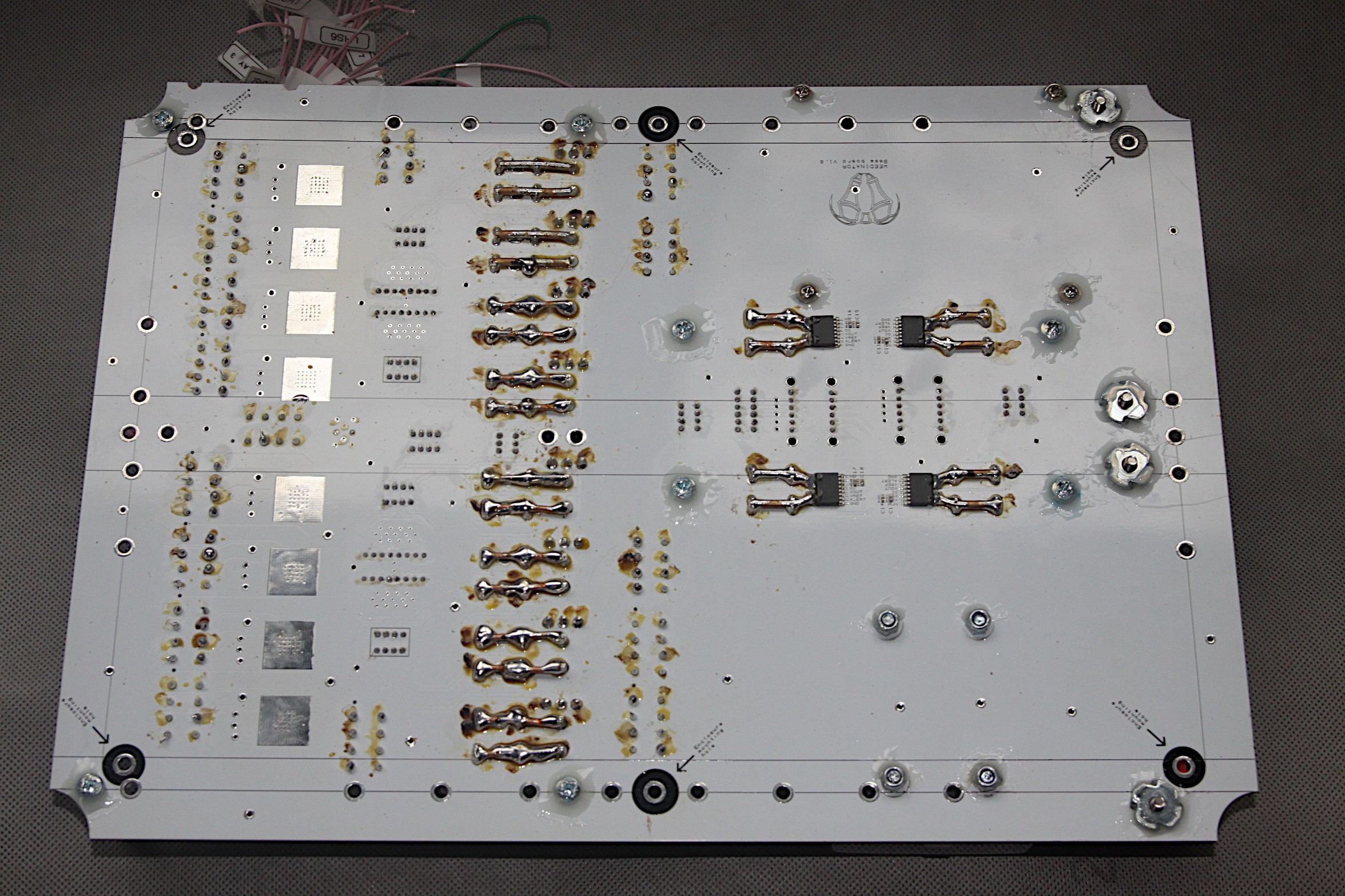
The four SMD chips on the right hand side are the current sensors. Liberal amounts of thread lock and pools of epoxy resin are used to help prevent the screws on the underside from coming loose. Some of the wiring is already started - the 3.3V logic - and it's now ready to be permanently installed into the enclosure box and some of the heavier wiring done. The current plan is to try and route a lot of the wiring to the far right hand side so that the main stack of PCBs can hinge on this side in case modifications need to be made. It's the same side as the antennae connections at the very top of the main PCB stack.
Discussions
Become a Hackaday.io Member
Create an account to leave a comment. Already have an account? Log In.