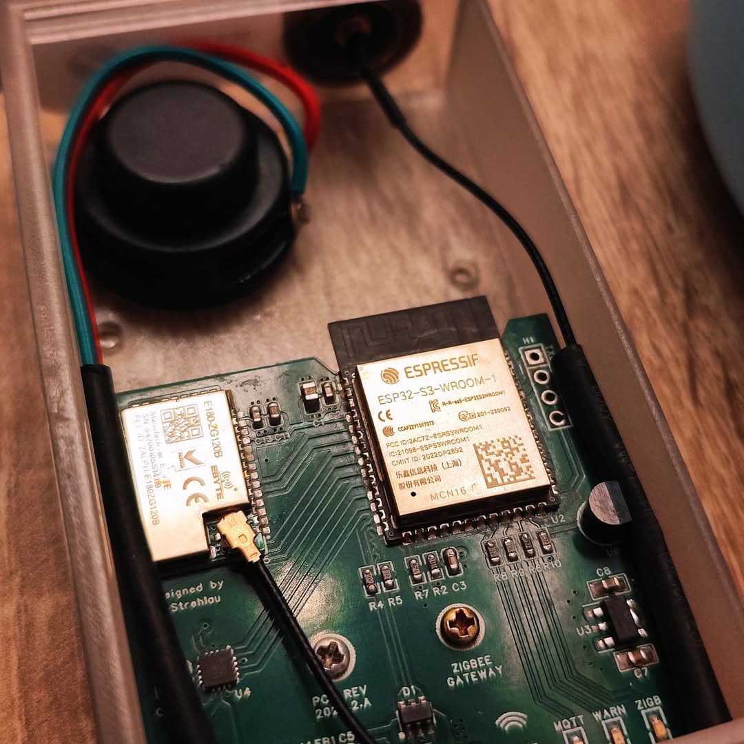
I recently revised the PCB design to enhance its structure and manufacturability:
- The stackup was modified to position the ground planes centrally, ensuring optimal signal integrity.
- The bottom layer was divided into two sections: 5V and 3.3V, each with its own dedicated ground plane for the signals.
- Only two traces are routed on the bottom layer: one for the delay circuit (soft-start for the ESP32) and the other for activating the DAC circuit.
- A ground plane was added to the top layer, which does not affect the electrical performance but simplifies the manufacturing process.
- I also introduced a damper circuit to address potential issues related to the ferrite bead.
- Component values were adjusted, and all schematics and Gerber files were updated accordingly.

In terms of software, I implemented several changes, with a few key improvements as follows:
- The jingles (welcome, alert, and info tones) were updated to be more pleasant to the ear.
- The device no longer plays the welcome notification during app rotation (e.g., when WiFi reconnects after a router restart), which is particularly useful at night.
- Fixed issues related to voice notification playback.
- Introduced functionality to indicate active notifications via a blinking LED, controlled through MQTT in Home Assistant, based on the "persistent notification count."
The previous PCB has been operating flawlessly so far, reliably controlling devices in the home. The new version performs just as well!
Lastly, I’d like to share that the project was also featured in an article on Hackster. Thank you for discovering and mentioning it — it's incredibly motivating! Thank you, Gareth!

If you want to read the article click here to read it on Hackster!
 h4rdc0der
Discussions
Become a Hackaday.io Member
Create an account to leave a comment. Already have an account? Log In.