teardownit
-
From prototype to product creation
03/13/2024 at 02:17 • 0 comments![]()
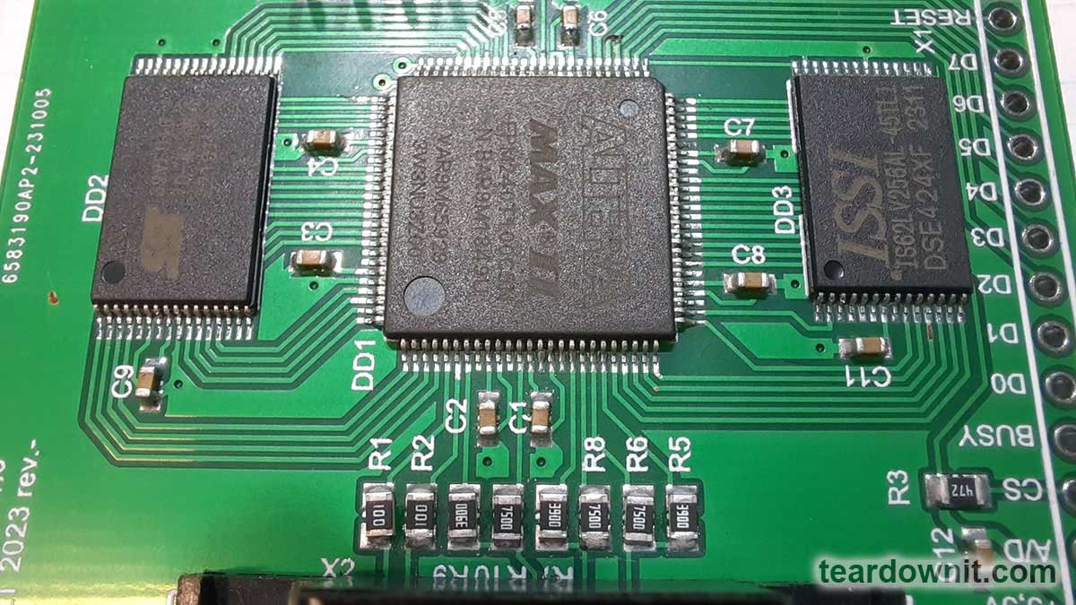
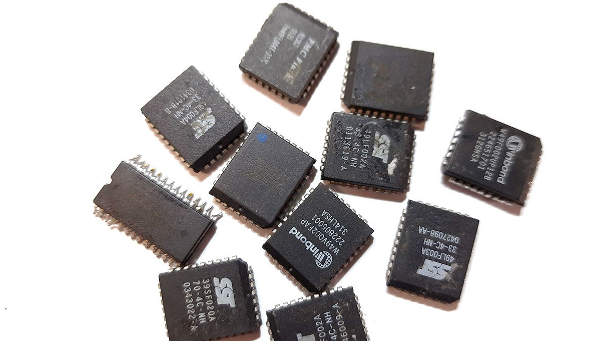
First of all, you should pay attention to the ROM used. The flash-ROM chip from an old computer motherboard has a finicky parallel interface where the address is written in two runs. This complicates the operating logic and increases access time. Additionally, the PLCC housing it comes in can be expensive and challenging to install manually. In this regard, it was decided to replace it with a more modern 39-series microchip from SST. These chips, such as the SST39LF and SST39VF, have faster access times (55 ns and 70 ns, respectively) compared to 270 ns for the 49 series chip. This allows one to reduce data preparation time to one cycle. The SST39VF010-70-4C-WHE chip has been ordered.
It is also necessary to replace the RAM. To save money, I picked one that operates precisely at 3.3 V and has TSOP housing. The IS62LV256AL-45TLI chip was ordered.
The CPLD chip remains unchanged.
![]()
These updates improve overall efficiency by reducing memory access times and using more convenient and modern components, which can also improve product availability and reliability in the future.
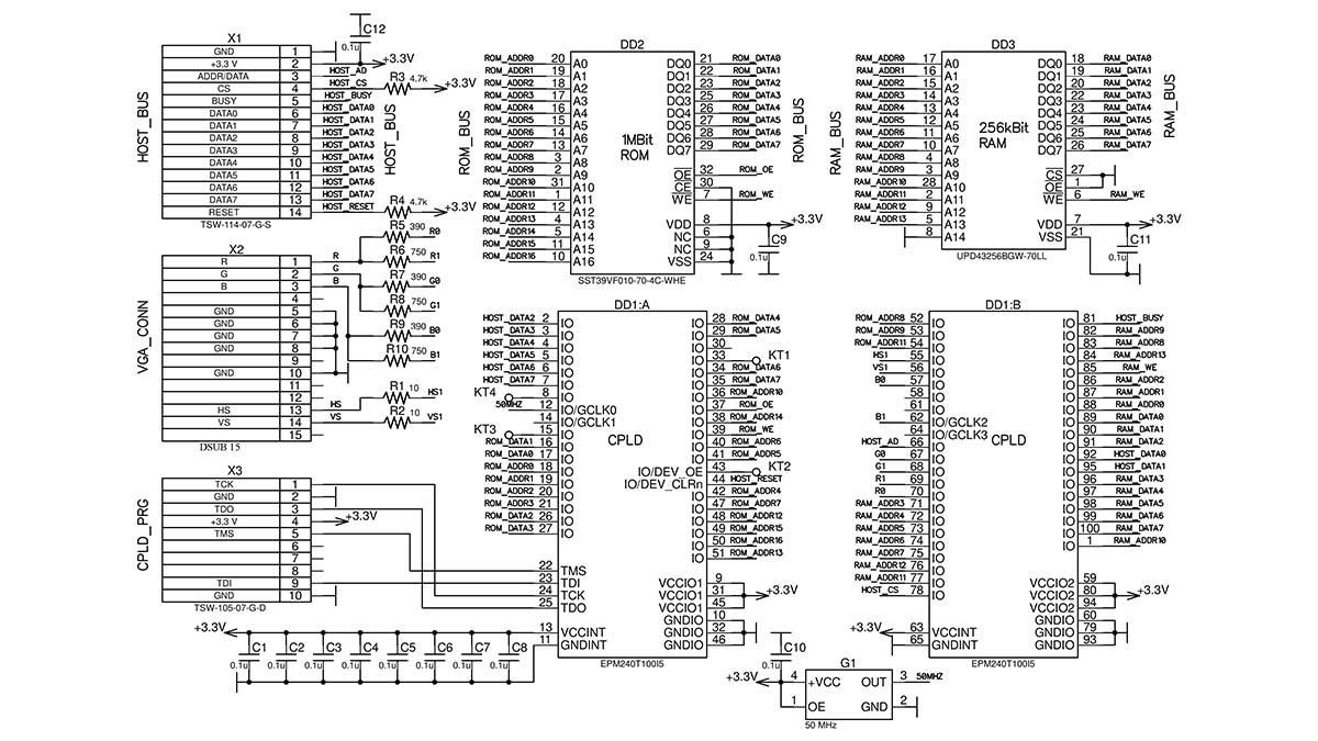
The updated diagram is shown below:
![]()
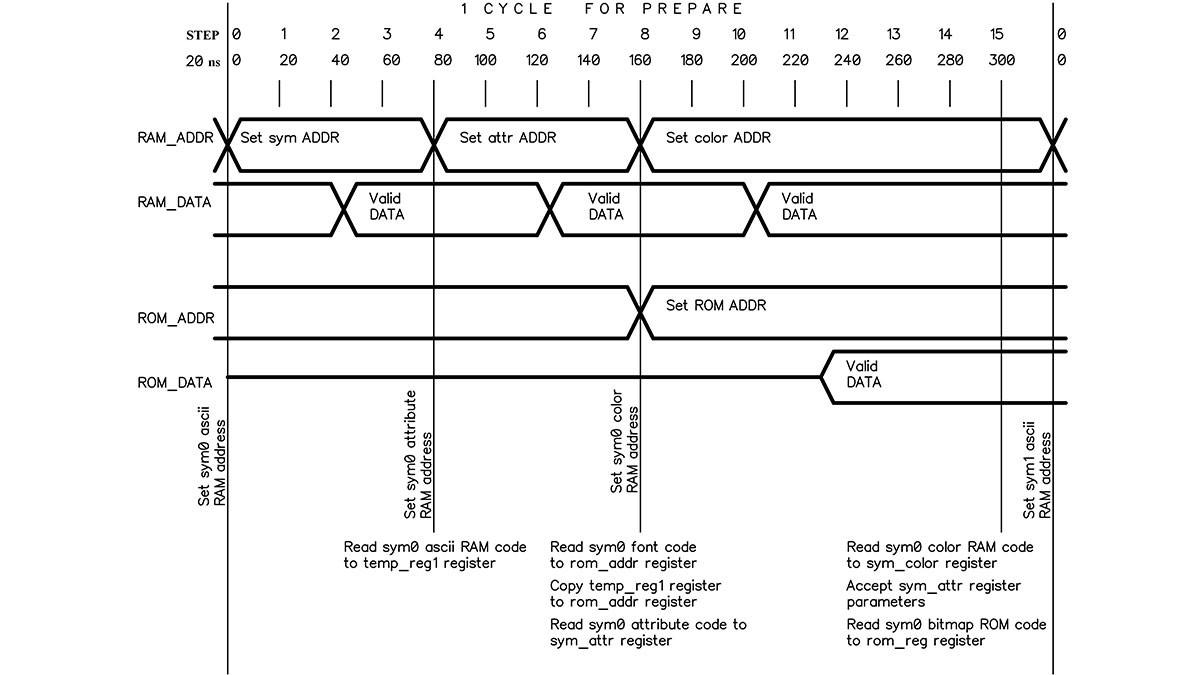
The timing diagram for new chips has become much more straightforward:
![]()
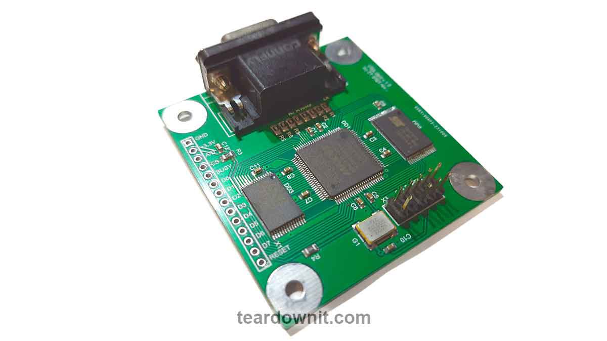
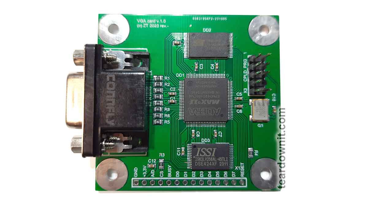
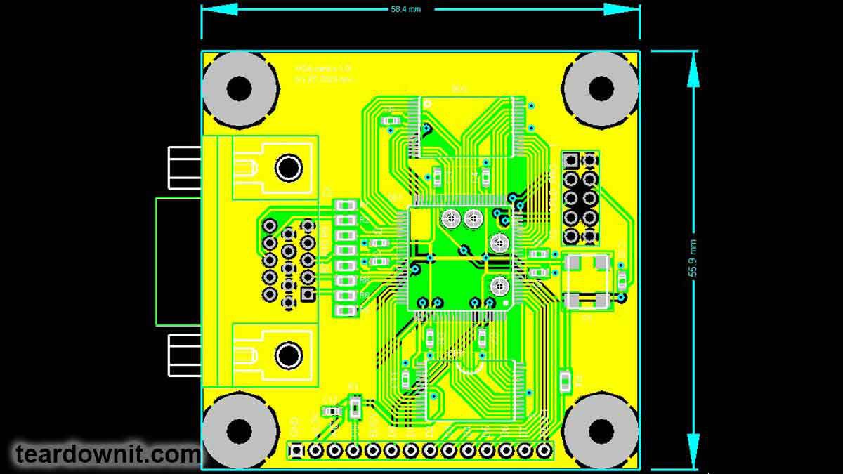
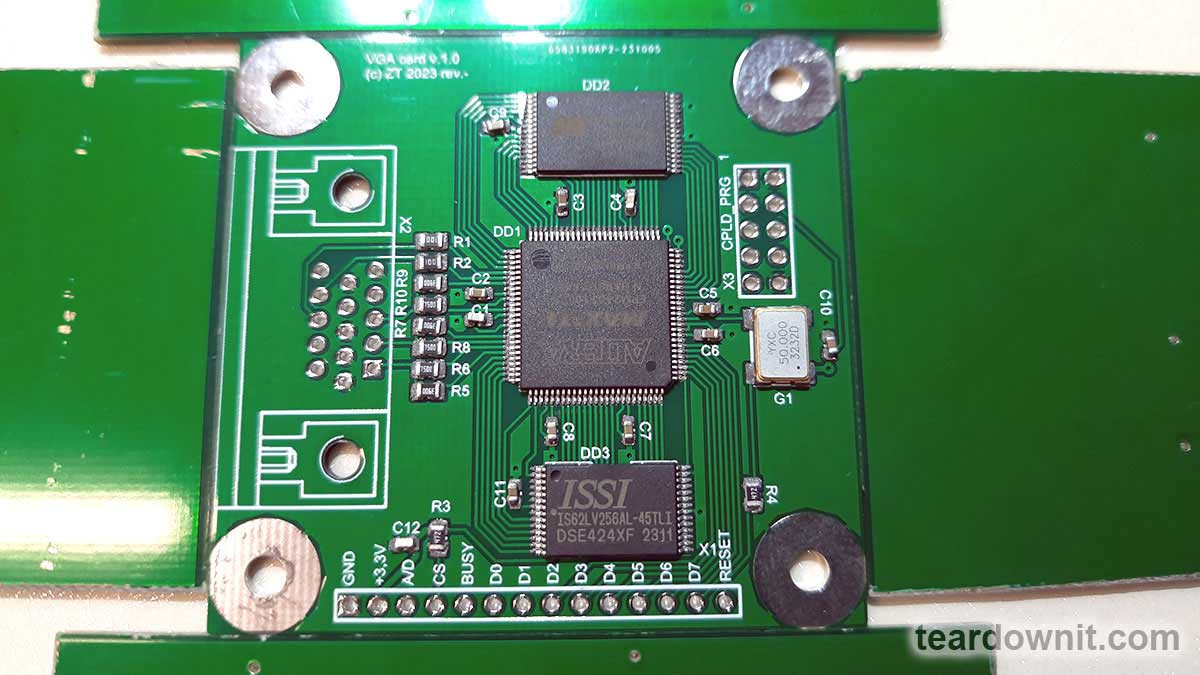
After the final selection of the main components, a printed circuit board, which had specific requirements, was created. The board had to be adapted for manual assembly. Due to this, components were placed on one side of the board, and the number of pinout components was minimized, leaving only external connectors.
![]()
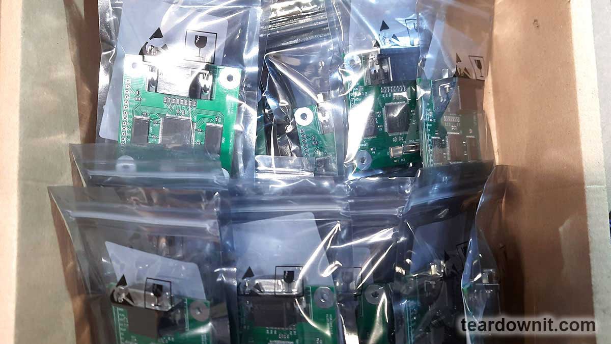
50 copies of printed circuit boards were ordered. This introduces the risk of the first boards' errors and inaccuracies, leading to scrapping all fifty and re-ordering the whole batch. Also, along with the boards, a stencil for applying solder paste was ordered. This will simplify the assembly process.
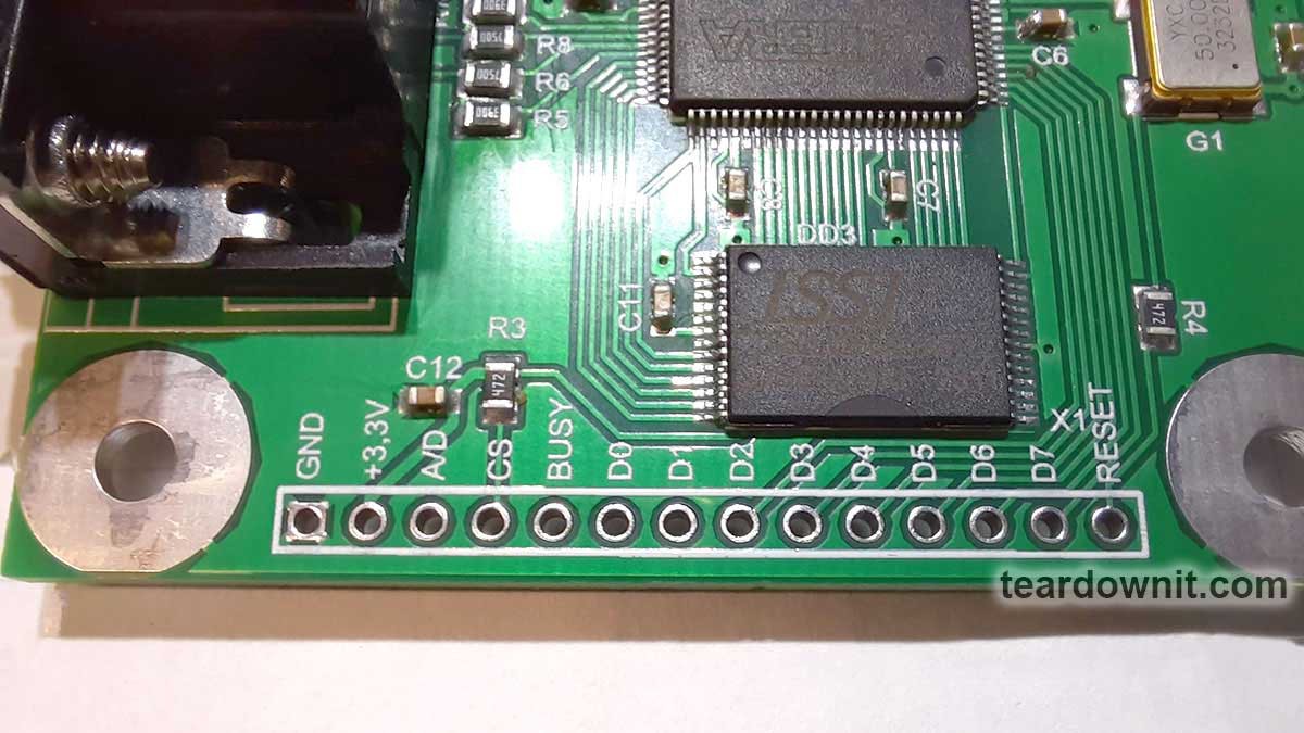
While waiting for the boards to be manufactured and delivered, it was time to think about flashing and testing the finished boards. Flashing CPLD was less difficult and could be done using a separate connector and USB programmer. However, programming the character ROM seemed more questionable. On a development board, to reprogram the firmware, the chip had to be carefully removed from the breadboard panel, inserted into the programmer, erased, flashed, removed, and returned to the breadboard panel. These operations turned out to be quite labor-intensive.
Therefore, to program the character ROM, it was decided to use the tools of the CPLD itself through a custom parallel interface. There were two possible implementation options:1. ROM programming with special firmware installed in the CPLD, intended exclusively for ROM programming.
2. Implementation of ROM programming functionality into the working CPLD firmware.The second option was more complex and required additional CPLD resources that would only be used once or twice in the device's lifetime. Fortunately, there were enough CPLD resources available to implement the second option.
![]()
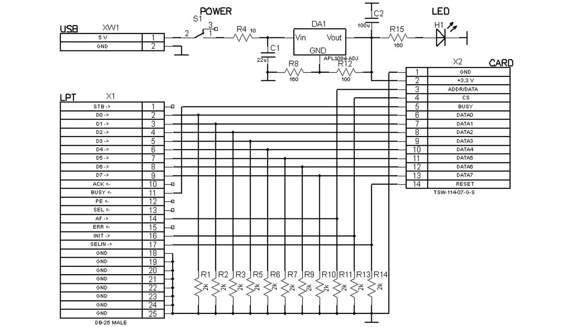
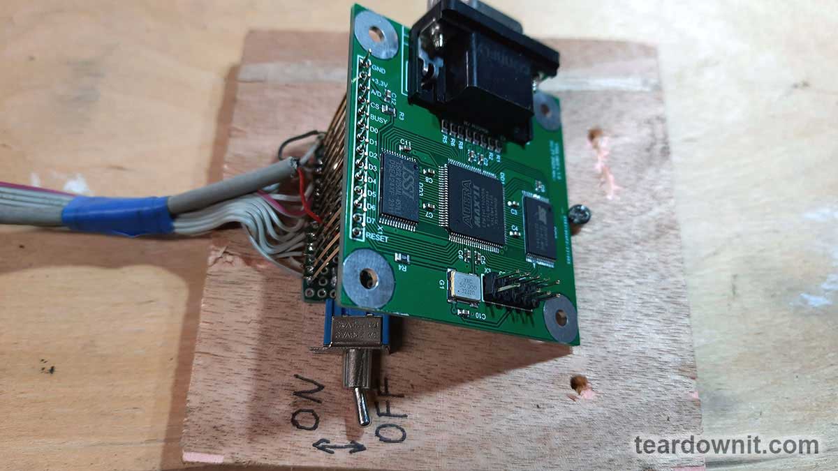
The finished prototype was tested through the same parallel user interface, displaying the test picture on the screen. To do this, I utilized an old laptop with an LPT port, which provided enough I/O lines to transmit all the necessary signals to the device.
![]()
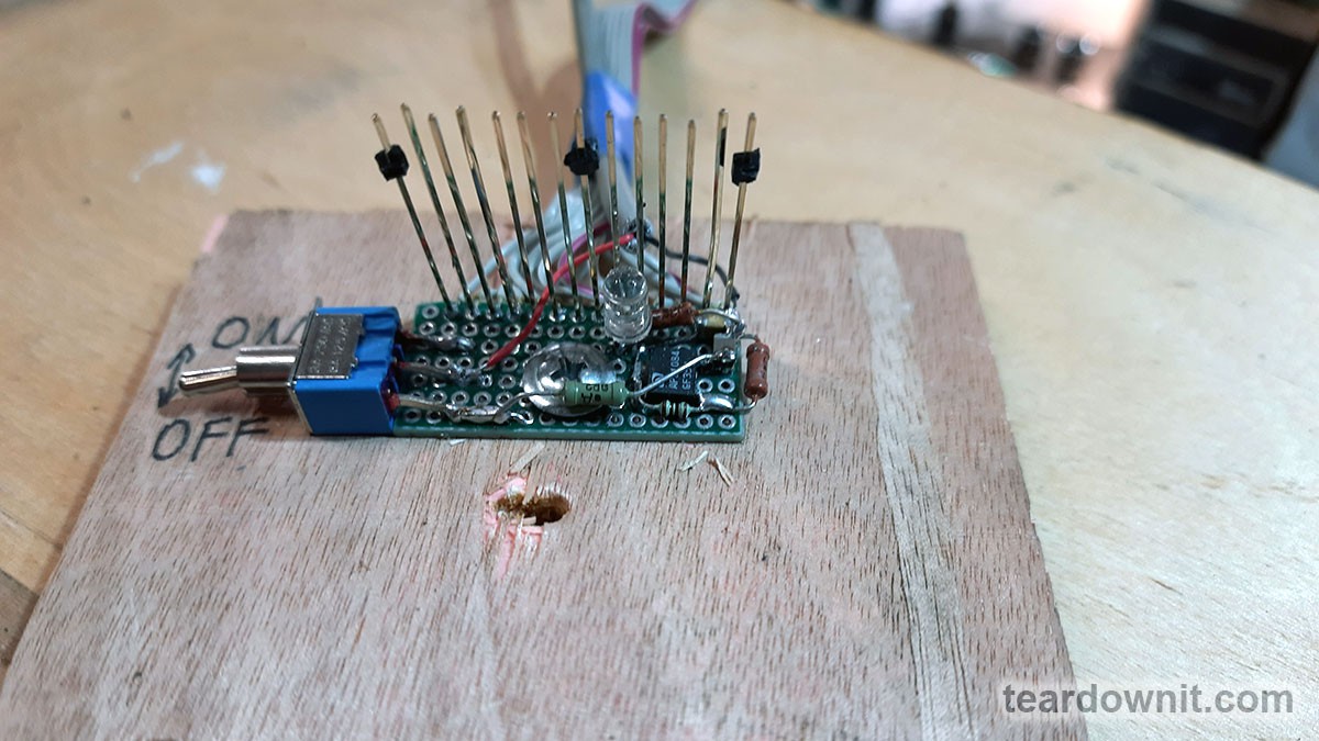
The testing device (diagram above) was assembled on a breadboard using the surface-mounting method. The resistors were installed in the housing of the DSUB25 connector, and the tested or programmed board was connected with long and flexible pins.
![]()
When bending, the contacts create tension in the board hole, ensuring reliable contact. 2 kOhm resistors, together with pull-up resistors of the LPT interface (approximately 1 kOhm), form a voltage divider. This divider converts the 5V logic levels of the LPT port to 3.3V ones.
The board is powered through a simple linear stabilizer, getting a voltage of 5 V from the laptop’s USB connector. Resistor R4 with a resistance of 10 ohms is used for current protection. Suppose a short circuit or other problems are on the board under test. In that case, its voltage will decrease, preventing the USB port from overloading. An LED controls a voltage drop of less than 2 V; it will not light up when the power is turned on.
![]()
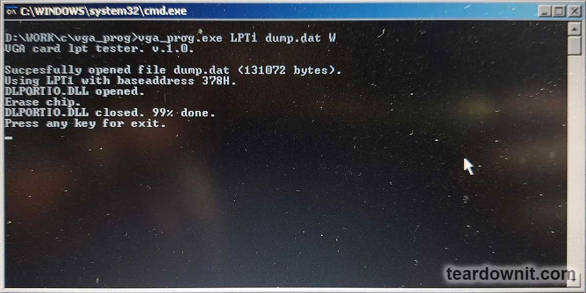
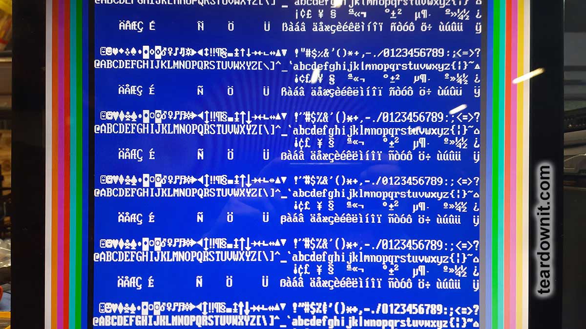
The command-line script for flashing the firmware and testing is written in C. For hardware access to the LPT port, the well-known DLPORTIO drivers are used. It should be noted that these drivers only work fine on Windows XP.
![]()
Font files are required to create a dump that will be written to the character generator's ROM. *. FNT files from the MSDOS system or programs of that time are suitable for this. These files contain bit masks of ASCII table characters. For example, in an 8x16 font, each character is described by 16 consecutive bytes.
![]()
Modern *. FNT files (as introduced into Windows systems) have a slightly different format. To extract bit masks from them and convert them to the desired format, the script fnt2bin.exe was created. This program takes as input a *. FNT font file with a height of 16 pixels. To convert any other font to the *. FNT format, you can use any free font converter. The result of running the fnt2bin.exe program will be a file of exactly 4096 bytes containing bit masks of the converted font characters. Thus, a dump of the character generator ROM firmware was created, including 32 different fonts.
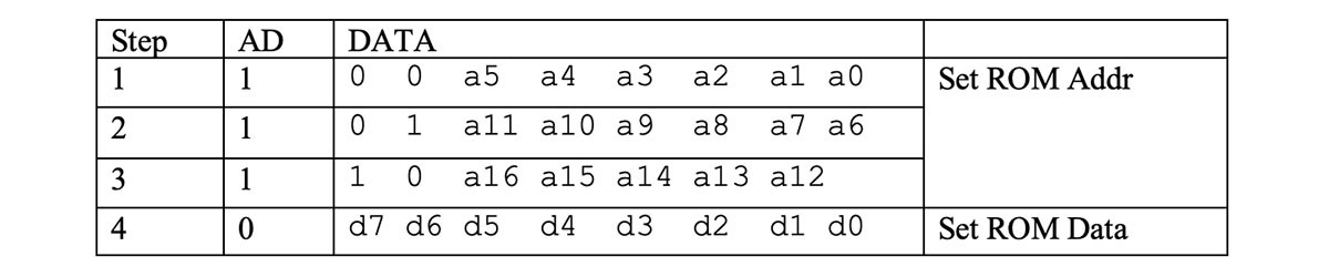
To flash this dump into the ROM using CPLD tools, one of the free bits of the control register was allocated. This bit can only be activated when a RESET signal is present. Upon exiting reset mode, this bit is automatically reset, returning the CPLD to regular operation. After setting this bit, the address setting logic changes, and this address register connects itself to the ROM address bus (not RAM). A 17-bit address is formed in three parts: 6, 6, and 5 bits. The two most significant bits of the address byte determine the "chunk" of the address being written: 00: bits 0 to 5, 01: 6 to 11, 10: bits 12 to 16. Then, one needs to switch to data transfer mode and transfer the data byte written to the ROM chip at the leading edge of the HOST_CS signal. Thus, one packet of address and data to the ROM chip consists of four parts, as shown in the table below.
![]()
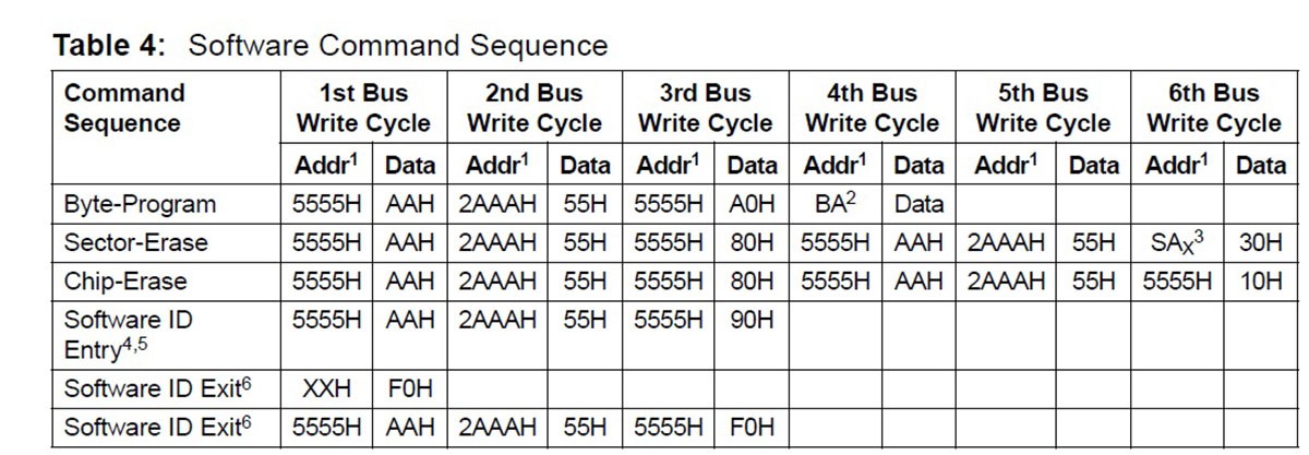
These messages then form sequences to initiate the byte's flashing. According to the datasheet, there is no "flash completion" flag; it is just waiting for a pause that clearly exceeds the time required for the firmware to flash.
![]()
The process is slow, but there is no point in rushing when flashing ROM since writing to the ROM itself takes a lot of time. Additionally, writing to the ROM is typically done only once per device.
During software development, the ordered boards, components, and chips arrived. A homemade device was created for applying solder paste. It has a sturdy laminated wood base with stops from PCB scraps to hold the board in place.
![]()
The stops were attached with thin, double-sided tape. A sheet of paper placed under the PCB being processed compensated for the height of the tape. This way, the board became perfectly aligned with the stops.
A stencil is placed atop the stops, and solder paste is applied.
![]()
The components are then placed by hand on the applied solder paste.
![]()
Positioning the components precisely is unnecessary since they will drift to their respective places due to surface tension during reflow and become nicely aligned. Although solder paste will stick components to the board, care must be taken not to accidentally dislodge already installed components.
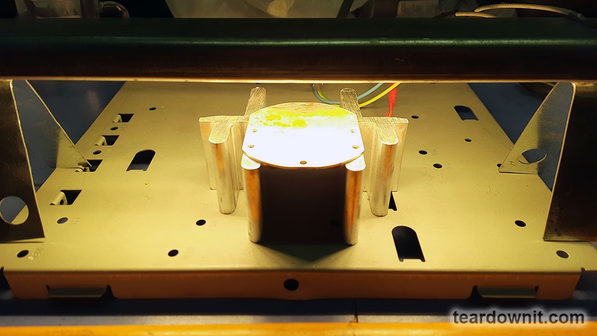
Solder reflow is performed using another homemade device.
![]()
It includes an aluminum heater based on a 300 W thermistor from AliExpress and an IR lamp from the grill of a faulty 600 W microwave oven. Melting occurs very quickly, literally within a few seconds.
![]()
During reflow, it is essential to keep a close eye on the components and, if necessary, use tweezers to help them move into place, especially if they are not attracted to their pads. If a solder bridge forms on two pins of a chip with a fine pitch, it must be removed using copper braiding.
After soldering the surface-mount elements, installing the output elements, such as two connectors, is time. After soldering, a visual inspection is performed, and the remaining flux should be washed off.
![]()
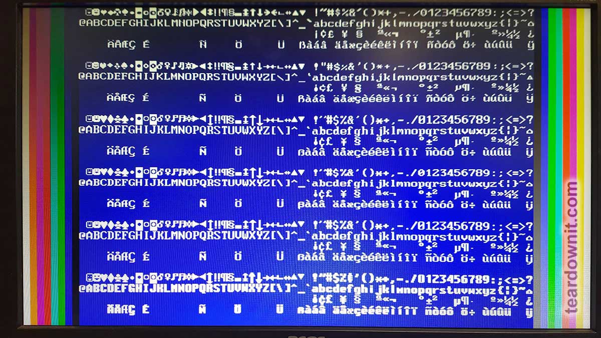
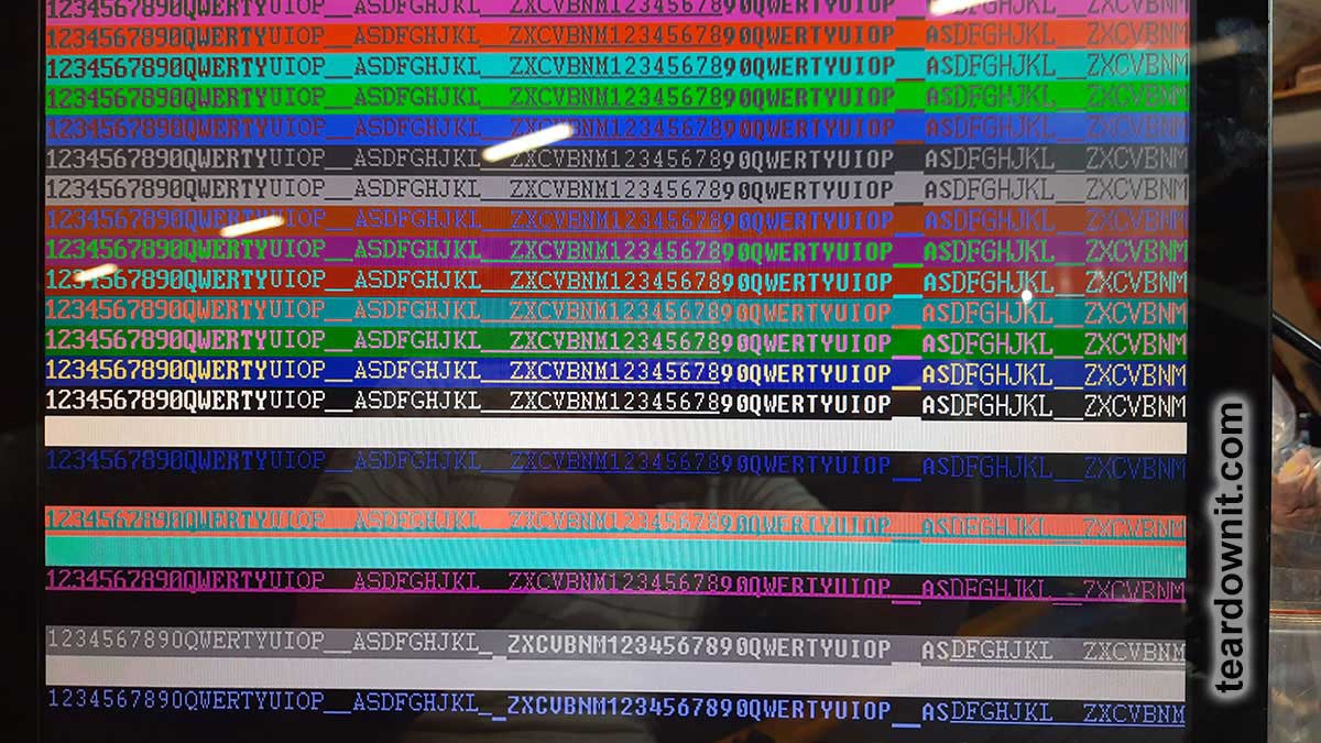
After these steps, the board is installed into the fixture for programming and testing. The test picture is shown in the photo below.
![]()
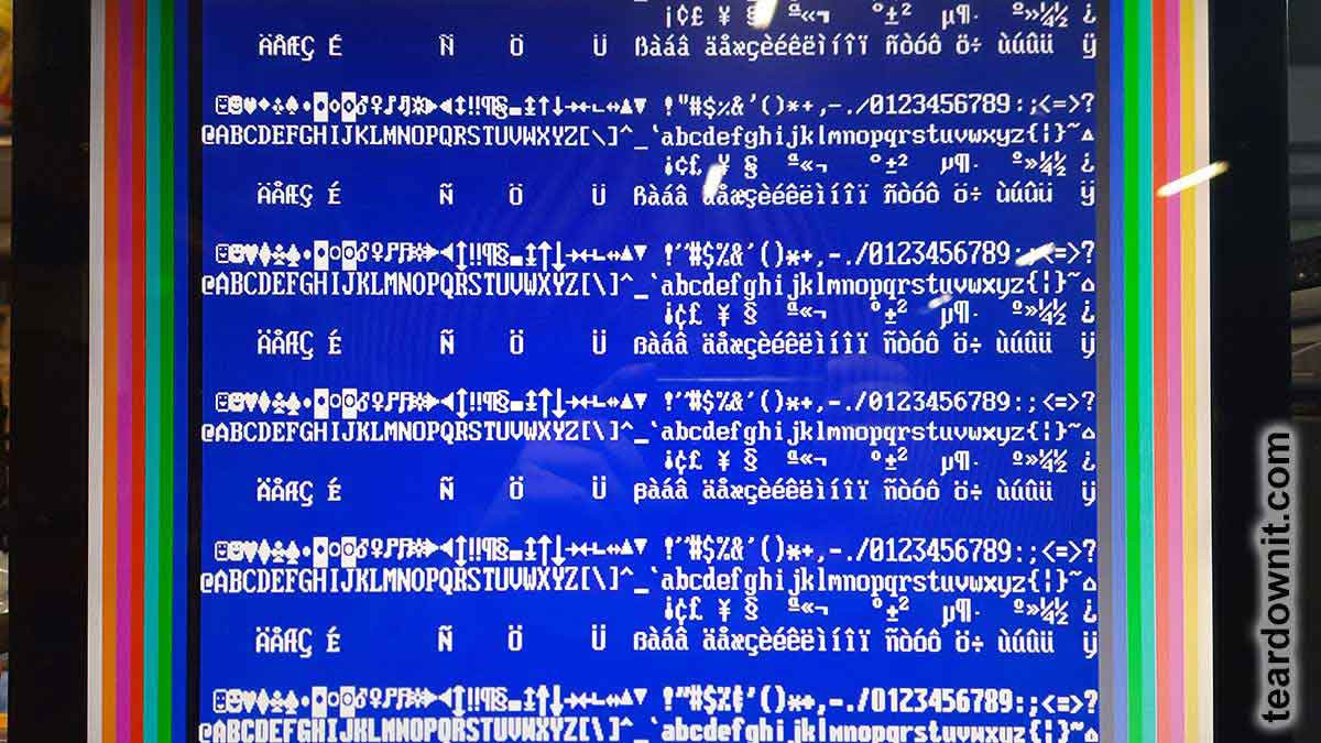
After removing the pin shorts and cleaning, it became evident that only 7 out of 20 boards worked. The rest required a more careful inspection for shorts and problematic soldering connections. As a result, 19 boards started working successfully. Still, one board had to be disassembled and reassembled on a new circuit board, and only then was it operational.
![]()
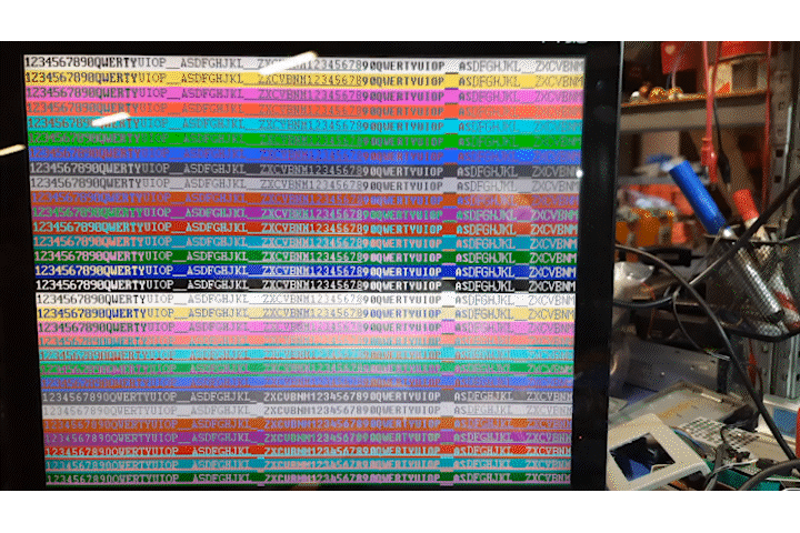
While working on the board, another idea arose: to use all the device's RAM for 128 characters in 32 lines. This mode would look better on widescreen monitors. This is what the test picture looks like on a widescreen monitor—too much horizontal stretch.
![]()
A temporary firmware was written for CPLD for testing, implementing a non-standard 1024×576 mode. This mode is not on the list of standard supported resolutions.
The horizontal parameters were taken from the 1024×768 43 Hz mode and the vertical parameters from the 768×576 60 Hz mode. At a pixel frequency of 50 MHz, the horizontal frequency was 39.55696 kHz, and the refresh rate was 66.25957 Hz. Both of these values are within the acceptable range; for example, the Acer V196HQL monitor, and this monitor displayed the image.
The photo below compares an area of 80×30 characters and an area of 128×32. The number of characters is 1.7 times greater.![]()
However, in this mode, 32 lines of characters use just 512 vertical pixels out of 576. Consequently, 2 lines at the top and 2 lines at the bottom of the image remain empty, and the characters themselves become small and less clear due to the discrepancy between the output and the monitor's native resolution.
![]()
Since this mode is non-standard, you cannot be sure it will work on all monitors. However, with a high probability, it can be assumed that there will be no issues if the operating frequencies fall within the permissible range.
The timing diagram for this version is:
![]()
-
Prerequisites and software
03/07/2024 at 15:05 • 0 comments![]()
Sometimes, when making your own devices on microcontrollers, there is a need to display huge amounts of information on a display and to use a bigger screen for ease of perception. Unfortunately, there are no ready-made and budget-friendly solutions for this task on the market. LCD displays with the ability to connect to a microcontroller are usually tiny and pricy.
But at the same time, there is a wide selection of legacy LCD monitors with a VGA interface. Models with a diagonal of 15 to 19 inches can be purchased in perfect working condition for a very low price, or one can even get one for free. This especially applies to monitors with a 4:3 aspect ratio. In addition, such models are usually quite reliable.
Most older monitors only have a VGA connector for connecting to a computer. Sometimes there is an additional DVI port (on more expensive models). The HDMI connector is more common on modern devices.
Thus, with a probability close to 100%, we'll get just a VGA on an older monitor. In order to display an image on such a monitor, it is enough to work with only five signals: analog R (red), G (green), and B (blue), responsible for the brightness of each color component, as well as digital HS (horizontal sync) and VS (vertical sync), providing synchronization. Analogue signal levels should range from 0 to 0.7 V, where 0 V corresponds to no light at all and 0.7 V to maximum brightness. Digital signals HS and VS are short pulses with a TTL level of negative polarity. The timings of these signals can be found, for example, here: http://tinyvga.com/vga-timing/640x480@60Hz.
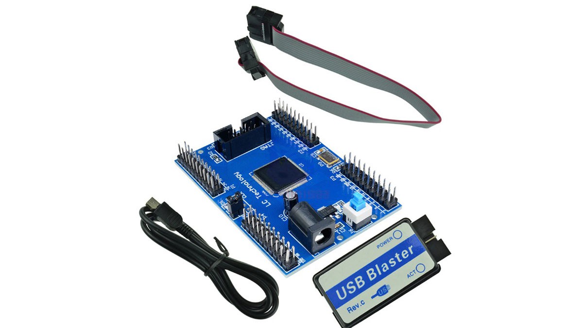
Typically, special controllers, or FPGAs, are used to generate video signals, and many FPGA development boards are already equipped with a VGA connector. However, FPGAs are often expensive and require many additional components. I was looking for a simpler and cheaper solution. As a result, the decision was made to use CPLD. CPLDs have fewer available logic gates (LEs) than FPGAs but are less expensive. For example, the MAX II Altera EPM240 development board is sold on Aliexpress: https://www.aliexpress.us/item/3256804686276488.html for only $8.12 (excluding shipping), and the kit even includes a programmer. The chips themselves can be purchased for $1.6–2.1 (for nice knockoffs).
![]()
Plain text mode was chosen for implementation because it is easier for a slow microcontroller but at the same time quite informative. Some graphics elements can be implemented using pseudo-graphics symbols, as was often done in the days of DOS. The introduction of a graphics mode would require transferring a large amount of data from the microcontroller and additional efforts to create it, which is not always possible, especially for weak cores.
CPLD has a built-in Flash ROM (User Flash Memory block, UFM), which can be used as a character ROM. However, its capacity is very limited—only 8 kbit, or 1 KB. This amount of storage is only sufficient for characters with a resolution of 5×7 pixels, and only if we discard non-displayable, insignificant, and visually identical characters from the ASCII table. In addition, the use of UFM will require the use of logic gates (LE), of which there are already a few. Despite the attractiveness of this option, I had to abandon it and use an external ROM chip, which can be salvaged from an old motherboard. Choosing a microchip with a supply voltage of 3.3 V will eliminate problems with matching voltage levels for the CPLD. The capacity of such ROMs is quite large: 2, 4, or 8 Mbit, or at least 256 to 1024 KB, which allows one to store a large number of different fonts with a decent resolution of 8x16 pixels.
![]()
To store the screen image, you will also need a RAM chip. Let's estimate the approximate size required for this. If we plan on using an 8×16 pixel font on a screen with a resolution of 640×480 pixels, we will end up with 80 characters per line and 30 lines on the screen. Thus, saving the screen image will require 80 × 30 = 2400 bytes. This number is somewhat inconvenient because it is just slightly larger than the nearest power of two, 2048. The memory use in this case is inefficient—only 58%, since the next power of two is 4096. By the way, this is exactly why text mode with 80×25 symbols became popular since there are 5 fewer lines on the screen. In this case, only 2000 bytes of memory are needed, which easily fits into 2 KB.
However, modern memory chips have significant storage sizes, and saving memory is not so critical nowadays. Moreover, one can deliberately choose to waste memory in order to simplify the decryption logic and save CPLD logic elements. Then you will need at least 4096 bytes (2^12, 12 address bits), which can be divided as follows: 5 address bits are allocated to the row address on the screen (30 of 32 will be used) and 7 bits to the column or position address characters in the string (80 out of 128 will be used).
4096 bytes are required only for storing ASCII symbols. The same amount of memory will be taken by the symbol attribute page. Attributes must include character color (3 bits), background color (3 bits), underline, and blinking. So, a memory of at least 8 KB is required.
Of the most affordable options, the best one is static RAM (used as cache memory), also salvaged from old devices or motherboards. It should be noted that this memory can only operate at 5 V. However. If it is a CMOS-type memory, it can take 3.3 V, but this will require timing correction.
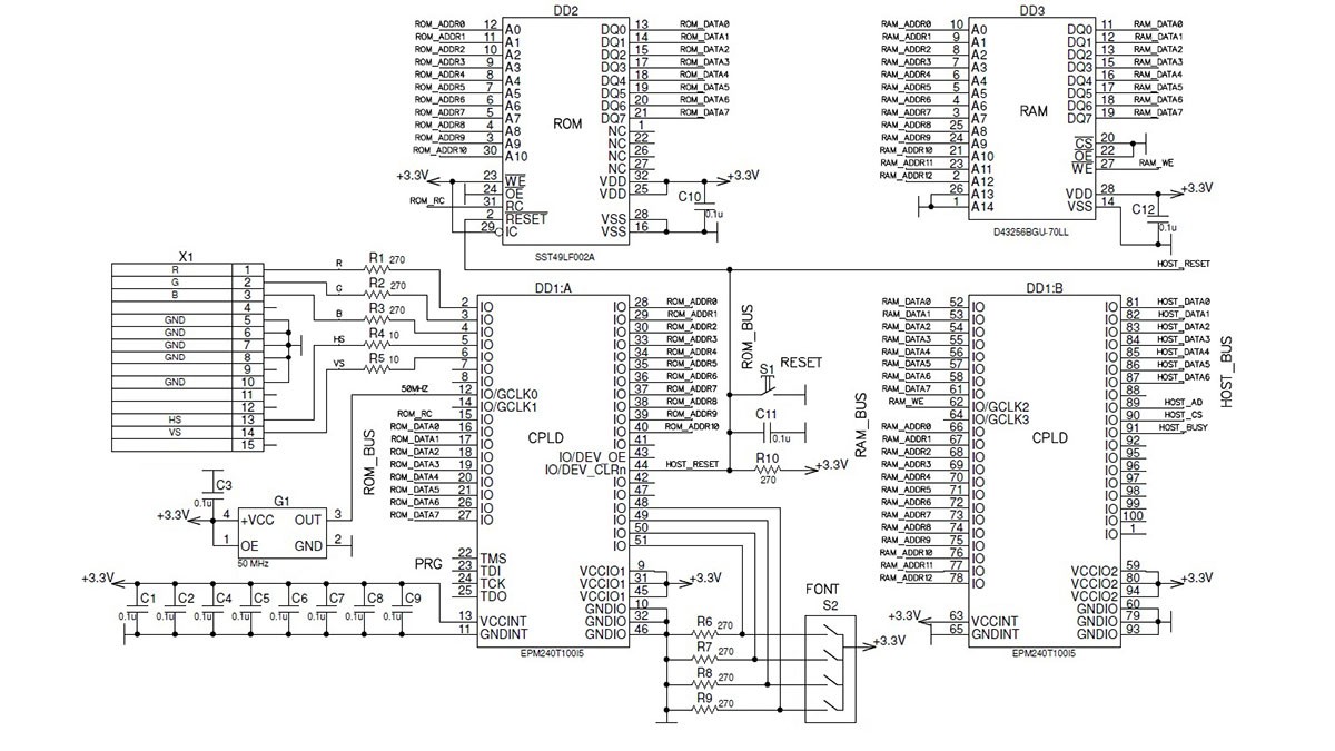
So, we got the following diagram:.
![]()
The circuit includes only three microchips and a minimum number of external components. Using the aforementioned Altera EPM240 development board as a base, all you need are ROM chips, RAM chips, and a DSUB header with five resistors. Connecting signals to the CPLD is just an approximation, since almost all of its pins are equivalent (with the exception of Global CLK, one of which requires connecting a signal from a clock generator). When the chip is repeatedly reprogrammed for a new device, almost all of its signals can be reassigned. Currently, the device is assembled on a breadboard and can be left aside.
The device communicates with the microcontroller via a parallel 8-bit interface (in the diagram, signals with the HOST prefix), which is logically almost identical to the widely used display interface on the 1602 and similar controllers. The only difference is the addition of a BUSY signal directed from the device to the microcontroller. Its necessity is due to the fact that access to the RAM chip is provided only during the backward sweep period. The rest of the time, the chip is busy (pun intended) executing CPLD logic. The BUSY signal also acts like an interrupt request (IRQ) function. When it's changed, the controller can automatically start writing to the screen buffer.
Interface description:
DATA[7:0] – eight bits of data, unidirectional port, intended exclusively for writing to the device
CS – chip select; 0 for chip is selected, 1 for chip is not selected. On the positive edge of the CS signal, the data is latched for writing.
AD – address/data, during a write operation: 0 – data is being transferred; 1 – address is being transferred.
BUSY – device busy state; 0 – free; 1 – busy. If the device is busy, the write operation to RAM is ignored. Writing is only possible to the address register.
RESET – device reset. 0 – reset; 1 – work. A hard reset can be used to turn off the screen immediately. When this signal is activated, the image output to the monitor stops. Resetting does not affect the contents of the RAM chip.
Writing data from the microcontroller to RAM is possible only during the backward sweep of the frame scan, when the RAM chip is not occupied by the CPLD logic. This time interval is 1.440 milliseconds. Despite the significant duration of this interval, when using slow microcontrollers, there may not be enough time to completely rewrite the entire memory space. For example, an AVR microcontroller, when operating at a frequency of 11.0592 MHz, is capable of recording only three full-screen lines with all the attributes. If one does not update the attributes (as is usually the case in real-life applications, attributes are written once when the program starts), then six full rows can be written in this time. Perhaps optimizing the code and rewriting it in assembly language can significantly speed up the process of updating data. Otherwise, it may take from 5 cycles (if updating only the data) to 15 cycles (if updating the attributes) to completely rewrite the screen. At 60 fps, it will take 1/12 to 1/4 of a second. Those who have ever worked on IBM PC/XT or IBM PC/AT computers with processor clock speeds around 4 to 12 MHz may notice the experience of refreshing the screen to be familiar.If you don’t want to wait for the next vertical pulse and want to record all the data at once, you can use the RESET signal. When activated, the internal logic of the CPLD stops and is disconnected from the RAM chip, allowing the microcontroller to directly access the memory. Registers for working with RAM are not affected by the reset signal.
In general, the write operations are as follows: you need to wait until the BUSY signal becomes zero, then put the desired data on the data bus, set the data type (address or data) AD, and set the CS signal first to 0, then to 1. When this signal changes from 0 to 1, the data is stored in memory. During a vertical pulse, the RAM chip is directly connected to the microcontroller's HOST signals, so maintaining the timings during writes becomes the responsibility of the microcontroller. However, since static RAM is a fairly fast device and typically has timings significantly smaller than the maximum speed of an average microcontroller driving its I/O lines, this task is not difficult.
The RAM chip D43256BGU-70LL is connected to the CPLD's output pins, with the lines having a 'RAM' prefix on the diagram. These signals include an 8-bit bidirectional data bus and a 13-bit address bus. Of the control signals, only the WE signal is used. Since there is only one chip on the RAM bus and both buses (address and data) are completely under its control, the OE and CS signals are not used, equal 0, and connected to GND.
The SST49LF002A ROM chip is connected similarly (signals with the 'ROM' prefix), except that the data bus in this case is unidirectional. The OE and WE signals of this IC are also not used and are directly connected to 0 (GND) and 1 (VCC), respectively.
Jumpers are connected to the available CPLD pins to select the current font. Since the ROM chip is large enough, it allows one to store several different fonts, including national alphabets, and switch to them by installing jumpers.
The DSUB VGA port is connected to the CPLD using only 5 resistors. Resistors in the HS and VS circuits are primarily for protection and can be ditched. Resistors in circuits R, G, and B are selected in such a way that, together with the input resistance of the monitor (75 Ohms), they form a voltage divider that reduces the voltage at the monitor input to 0.7 V.
The power leads are shunted with ceramic capacitors, and the clock signal with a frequency of 50 MHz from a crystal is supplied to the GCLK0 pin. These parts were on the breadboard originally.
A resistor, a capacitor, and a button are connected to the RESET signal, forming it. However, if the signal is generated by a microcontroller, these components are redundant.
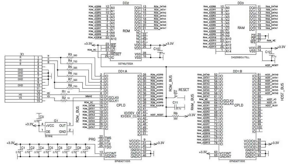
After creating the main part of the CPLD operating logic, it became clear that the number of logic elements (LEs) used was slightly over half of the available ones. In this regard, the idea arose to complexify the logic and add more features. First of all, the number of colors can be increased to 16 by adding three additional CPLD pins and three resistors. This won't significantly complicate the scheme, but it will add eight more colors. In this case, the RAM page with attributes will have to be completely devoted to color, and another page with attributes will have to be added, increasing the RAM address bus by 1 bit. In the second page of attributes, you can implement font selection, underlining, character and background flickering, and so on.
The new scheme looks similar to the previous one.
![]()
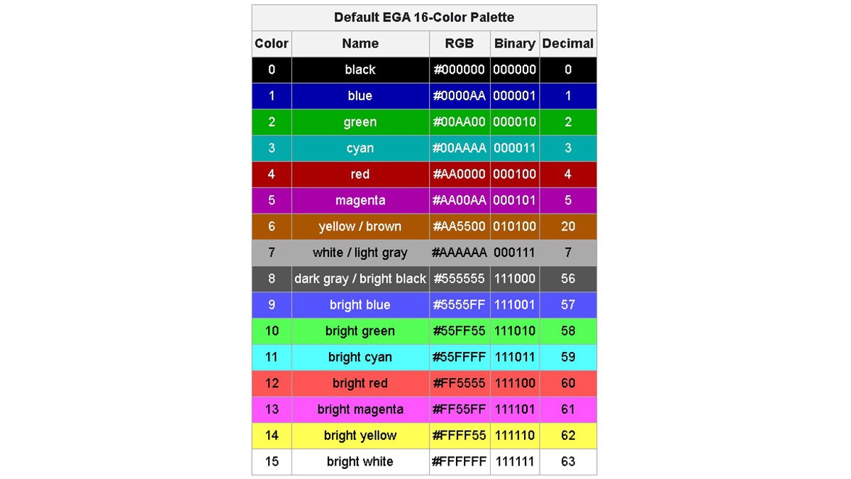
As the number of colors increases, the question is: which palette to choose? With only 8 colors, there is no such question; all colors are different combinations of the three primary colors: red, green, and blue (2^3 = 8). When there are more colors, different options are possible. For example, the 16-color EGA palette: https://moddingwiki.shikadi.net/wiki/EGA_Palette:
![]()
As can be seen from the presented palette, the 4th bit in the color number stands for brightness. However, the halves of the table are not evenly separated by brightness. The first half is set to 2/3 brightness (byte AAH = 170 = 2/3 × 256). In the second half, another 1/3 of brightness is added (byte 55H = 85 = 1/3 × 256), and the colors in this part are called "bright."
Interestingly, color No. 6 (yellow/brown) in this scheme deviates from the expected AAAA00 and is specifically set to AA5500. This was done to replace the unattractive, dirty yellow color with the more appealing brown. This is a known feature of EGA video cards and monitors. Some monitors took this into account, while others did not implement this feature in order to simplify the circuit. Some models added a BROWN ADJ knob so that the user could set the desired shade of that color. That is why the color in the table is indicated as yellow/brown.
Nonlinear separation by brightness level automatically leads to two shades of gray showing up: light gray and dark gray, which are widely used.
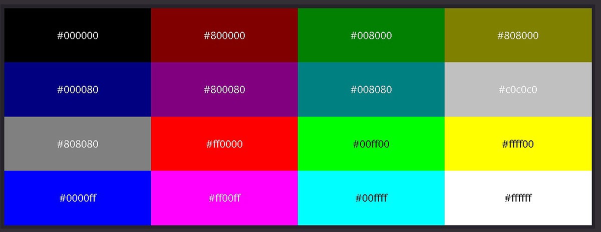
In the 16-color VGA palette: https://lospec.com/palette-list/microsoft-vga, the situation is slightly different: the colors are divided exactly in two halves by brightness (80H = 128 = 1/2 × 256):
![]()
There is also a noticeable outlier in this palette: light gray (С0С0С0), which should be black, duplicating an existing color. Additionally, this color swapped places with the dark gray color (808080). This was done intentionally to ensure compatibility between the VGA and EGA 16-color palettes, making them almost identical.
In our case, when the R, G, and B signals are generated in hardware using resistors, it is more convenient to use the EGA palette. So, it is necessary to make a software correction only for one color, No. 6. All other colors are generated automatically. Switching to the VGA palette would require not only a program change but also an additional group of resistors to be added to create the light gray color (C0C0C0). The resistors should be picked so that one group provides a brightness level of 1/3, the second is 2/3, and together they provide full brightness. By simple calculations using Ohm's law, we get the following values: 390 Ohms and 750 Ohms.
The signal generation logic for a static image like the one with test color bars is quite simple. However, if it is necessary to generate a dynamic image, the task becomes more complicated. It is necessary to organize a logical interface with RAM and ROM. At the same time, data exchange should occur not just quickly but lightning-fast! Let's first evaluate whether the selected chips can keep up with operating like this.
So, the resolution is 640x480. Pixel output frequency is 25 MHz (the standard specifies 25.175 MHz, but rounding to 25 MHz is acceptable since VGA, like many other analog standards, allows a significant spread of parameters). The frame refresh rate is 60 Hz (actually 59.5 Hz), and the line refresh rate is 31.46875 kHz (actually 31.25 kHz). Thus, the output time of one pixel is 40 ns, and the output time of an 8-bit character is 320 ns. During this time, the ASCII code of the character (one byte), the color code (one byte), and the attributes (one byte) should be read from RAM, and then, using the ASCII code as an address, we should read the bit mask of the character from ROM. Only then will the CPLD logic have all the necessary information to begin imaging.
According to the technical description (datasheet), for the selected D43256BGU-70LL chip, a full read cycle takes 70 ns. Considering the use of the chip at reduced voltage, the read cycle takes longer—let's say, 100 ns. Thus, in 320 ns, we will have enough time to read three bytes from RAM: ASCII code, color code, and character attributes. Great. The situation with ROM is more complicated: the address is written to it in two steps—in rows and columns—and, according to the manual, the read cycle takes 270 ns. Not the highest speed, but within the required 320 ns, even with time to spare.
The problem is that we can't start issuing the ROM address until we know at least the ASCII code, which takes 100 ns. This sums up to 370 ns. What saves us is the fact that each RAM or ROM read cycle individually fits within the allowed interval, and we can simply spend two additional cycles reading data. To add these two loops during data preparation, it is necessary to shift the character display area, creating an additional blanking area 2 characters wide at the beginning of the line and reducing the same area at the end of the line by 2 characters. This is quite simple to do: we simply shift the horizontal blanking pulse by 640 ns (accordingly, the horizontal sync pulse also shifts). From the monitor's point of view, there is no difference.
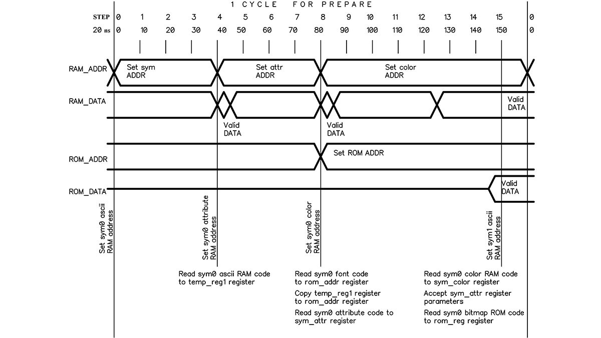
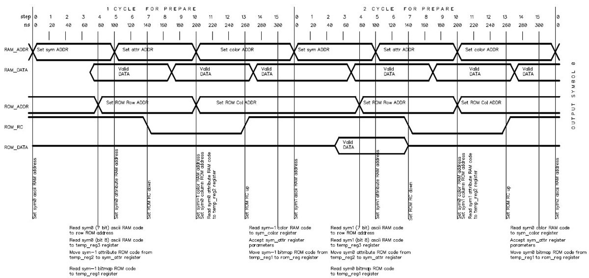
To better understand when and what to write and read, it is handy to create a timing diagram. At the beginning, all the timings were in my head, but creating a paper diagram and giving it another look allowed me to significantly optimize read cycles and even reduce the number of registers used.
![]()
The cycle begins by setting the RAM address of the ASCII character byte on the bus. After 80 ns, the requested byte appears on the RAM data bus, which is instantly used to generate the byte read address from the character generator ROM. At the 100 ns mark, we set the address of the symbol attributes byte to the RAM address bus. At 140 ns (60 ns after setting the address), we latch the first part of the ROM address. After another 60 ns, we set the second part of the address on the ROM address bus. At this point, there should be a byte of data on the RAM data bus with character attributes, where 5 bits correspond to the font and are included in the second part of the ROM address. The remaining 3 bits of data are stored in temporary register 2. After another 60 ns, we latch the second part of the ROM address. Data will appear on the ROM data bus 120 ns after this event, already during the second cycle. To prevent loop intersections, we write this data to temporary register 1 at 80 ns. And finally, at 300 ns, all the prepared data is written to the working registers. The character bitmask from temporary register 1 is copied into the rom_reg register, and the stored attribute bits are applied to the color byte that has been read at that time.
Thus, by the end of the second loop, all the data will be ready for outputting the symbol.
Writing data from the microcontroller to RAM is carried out as follows. We wait until the BUSY signal becomes zero, after which we set the starting addresses in the registers where data will be written. Typically, this is address 0, corresponding to the start of the data page, but a random address can also be chosen if only a few bytes need to be changed. Then we record the data. After each byte is written, the address is automatically incremented. When the edge of the screen is reached (the 80th character in a line), the address of the character position in the line is automatically reset to zero, and the line address is incremented by 1. After the entire page of data is written, the address is automatically adjusted to the attribute page entries and then the color page entries. After writing all three pages, the address is also automatically reset, and the process begins again with writing to the data page. Thus, the start address is set only once, and then only data is written. This saves a few microseconds on address setting and simplifies the code when all data can be transferred in one cycle.
Data format for writing data (AD=0):
![]()
The data page stores ASCII character codes.
![]()
The attributes page stores symbol attributes. The lower two bits are responsible for the hardware-driven blinking of a character or background, and the third bit is for the underline. The upper 5 bits select the font. Accordingly, you can display characters from different fonts mixed in any combination. 5 digits for selecting the font allow one to store 32 different fonts, which can include any symbols of national alphabets as well as tiles for displaying an image.
![]()
The color page contains the character color and the background color. Color can be anything from the 16-color palette.
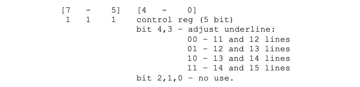
There are three address registers. The choice of which particular one to write to is defined by the most significant bits of the data byte. If the most significant bit [7] is 0, then the position register in the row (column) is written. If it is 1, then the line number register (line) and RAM page number register (ASCII code, attributes, or color) are written. If the three most significant bits are equal to 1, then a special control register is written, bits [4] and [3] of which determine the position of the hardware-generated line when the underscore bit is turned on, and bits [2–0] are reserved for future settings.
Data format for writing address (AD = 1):
![]()
A register stores the position in a string.
![]()
The register stores the line number and page selection.
![]()
If you set an address outside the range of 0-79 for a column and 0-29 for a row, then data will begin to be written to the shadow memory area, which is not displayed on the screen. There is nothing wrong with this; after passing the address 127, the data will again be written to the visible area.
Internal CPLD registers (some):
![]()
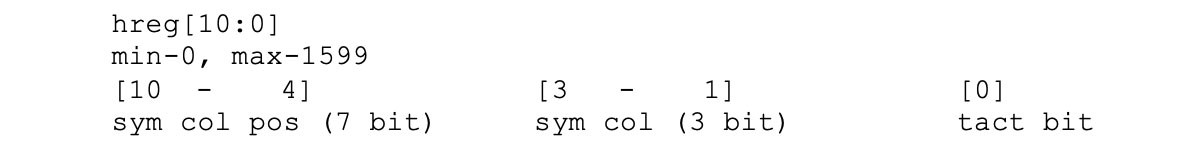
The register contains the current horizontal scan position. It is clocked at a frequency of 50 MHz, which is two times the required 25 MHz, so the least significant bit (tact bit) is not used. Accordingly, bits 1 to 3 indicate the position within the character, and bits 4 to 10 indicate the position of the character in the string. When the value reaches 1600, the register is reset to zero, and the value in the vreg register is increased by 1.
![]()
The register contains the current vertical scan position. Clocked from the hreg register. Bits 0 to 3 indicate the line within the character, and bits 4 to 8 indicate the line on the screen. Bit 9 is not used. When the value reaches 525, the register is reset to zero.
![]()
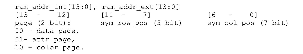
The registers contain the current address value for accessing RAM (16 KB in total). The lower 7 bits are the character address in the line (column), then 5 bits are the line address, and 2 bits are the page address (ASCII code, attributes, or color). There are two of these registers: one for internal use by the CPLD logic, and the second is controlled externally by the microcontroller.
![]()
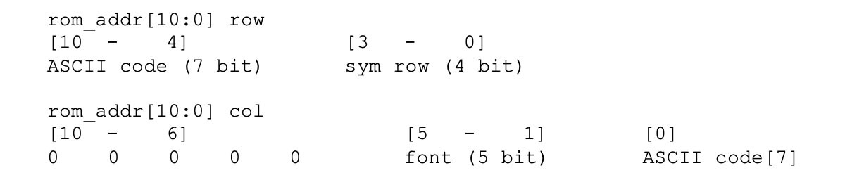
The ROM address register is written in two stages. It contains the character string address, the character's ASCII code, and the font address. These addresses are located in such a way that one can flash standard DOS *.fnt font files into the ROM without any additional processing, just one after another. You can combine several fonts into one file for firmware using any file editing program. Just make sure that the fonts have a resolution of 8x16.
![]()
Color output register. This register is connected directly to the CPLD pins, supplying the R, G, and B signals to the monitor. The lower 3 bits provide a signal with 2/3 of a brightness level (they must be connected to 390 Ohm resistors); the highest ones provide a signal with a brightness level of 1/3 (they must be connected to 750 Ohm resistors).
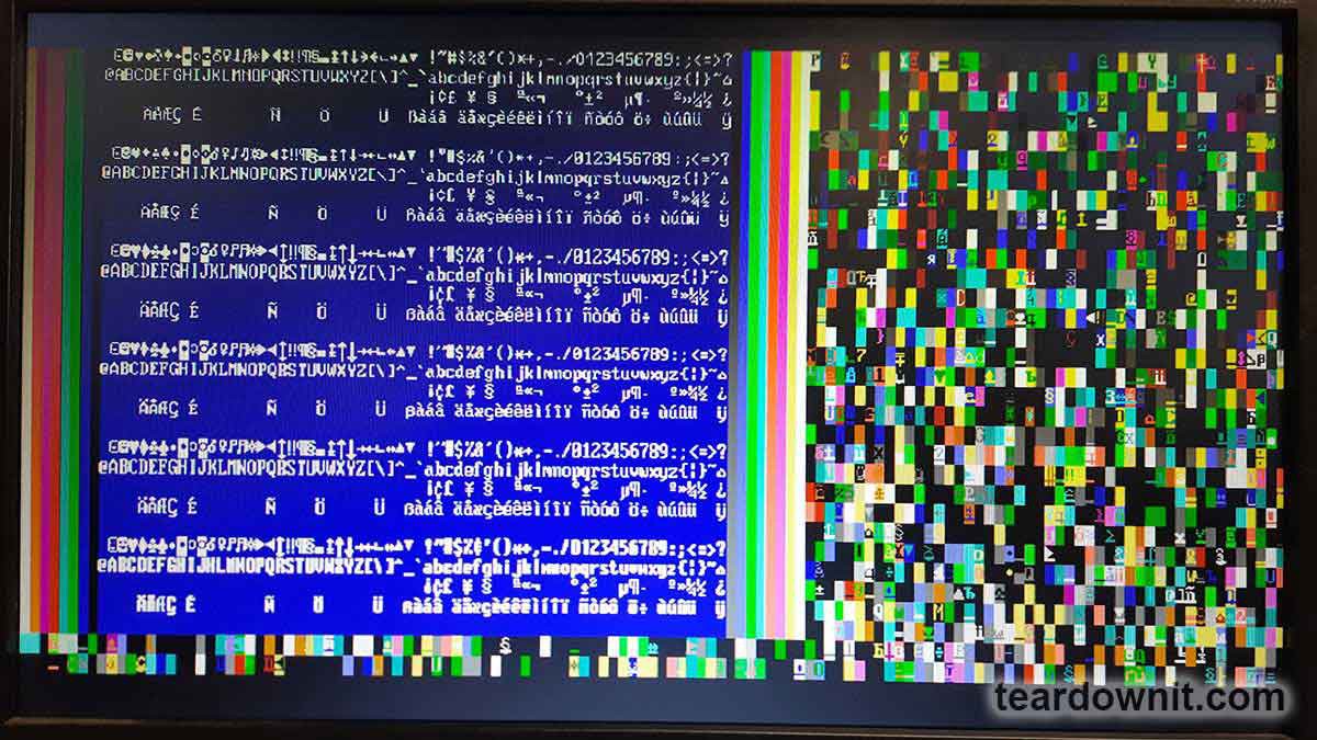
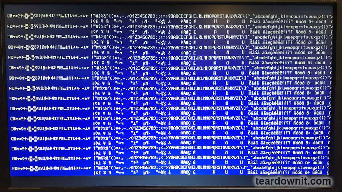
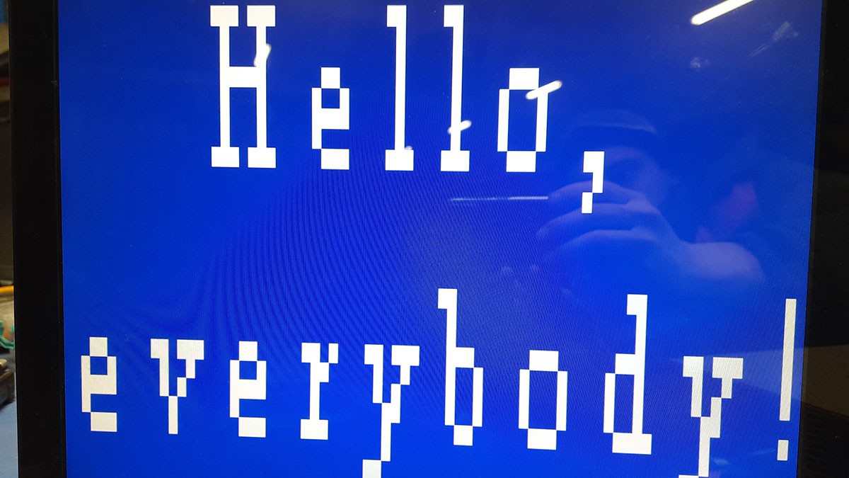
Photos to illustrate:
![]()
![]()
![]()
![]()
VGA videocard for microcontrollers
Creating a DIY videocard for microcontroller