 Ken Yap
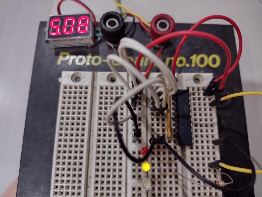
GAL (Generic Array Logic) is descended from PAL (Programmable Array Logic). At the beginning these were fused, then UV erasable, and then flash programmable.
A common use for PALs was to replace a lot of small scale logic in products like computer motherboards. GALs have displaced PALs so we won't discuss those any more. Current GALs are electrically reprogrammable.
My first well-defined task is to write a configuration for a BCD to 7-segment output decoder. I'm using the ATF16V8B. This has up to 16 inputs, 8 I/Os, and runs off 5V. Most of the programmable logic devices have moved to 3.3V. But this one is still in production and useful.
A GAL assembler is needed to take a specification of the logic and turn it into a JEDEC file which is a standard format for GAL programmers like the TL866. In the Windows world WinCUPL is well-known. In the *nix world, there is GALasm. More recently, Galette, a rewrite of GALasm in Rust has appeared. I'll be using this.
The specification language for GALasm and Galette is shown on this example page. The combinatorial logic for output terms is expressed as the sum of products of input terms. By De Morgan's rule this is equivalent to product of sums. Inversion is also available. This can generate any result from a combination of inputs. Let's jump straight into 7-segment logic.
GAL16V8
gal7seg

CLOCK I0    I1    I2    I3    NC    NC    NC    NC   GND
/OE   OA    OB    OC    OD    OE    OF    OG    NC   VCC

define(`B0',`/I0*/I1*/I2*/I3')dnl
define(`B1',`I0*/I1*/I2*/I3')dnl
define(`B2',`/I0*I1*/I2*/I3')dnl
define(`B3',`I0*I1*/I2*/I3')dnl
define(`B4',`/I0*/I1*I2*/I3')dnl
define(`B5',`I0*/I1*I2*/I3')dnl
define(`B6',`/I0*I1*I2*/I3')dnl
define(`B7',`I0*I1*I2*/I3')dnl
define(`B8',`/I0*/I1*/I2*I3')dnl
define(`B9',`I0*/I1*/I2*I3')dnl
define(`BA',`/I0*I1*/I2*I3')dnl
define(`BB',`I0*I1*/I2*I3')dnl
define(`BC',`/I0*/I1*I2*I3')dnl
define(`BD',`I0*/I1*I2*I3')dnl
define(`BE',`/I0*I1*I2*I3')dnl
define(`BF',`I0*I1*I2*I3')dnl

/OA = B1 + B4 + BB + BD

/OB = B5 + B6 + BB + BC + BE + BF

/OC = B2 + BC + BE + BF

/OD = B1 + B4 + B7 + BA + BF

/OE = B1 + B3 + B4 + B5 + B7 + B9

/OF = B1 + B2 + B3 + B7 + BD

/OG = B0 + B1 + B7 + BC

DESCRIPTION

A BCD to 7 segment decoder
You can see that it's shorter to express the output terms as the inverse of the sum of input terms, i.e. list the digits for which a particular segment is off.
I used the minipro software to flash this to the chip, as this Makefile shows:
#
# Uses GNU make for pattern substitution
#

default:        7segment.jed

%.jed:          %.pld
                galette $<

%.pld:          %.pldm
                m4 $< > $(<:.pldm=.pld)

%.flash:        %.jed
                minipro -p "ATF16V8B" -P -w $<
Galette takes .pld files so why the .pldm files? If you look at the specification, the input terms representing the 16 BCD combinations are repeated. So I used the m4 macro processor on *nix to save typing and reduce the chance of errors, the Don't Repeat Yourself principle. Here is the result of the preprocessing:
GAL16V8
gal7seg

CLOCK I0    I1    I2    I3    NC    NC    NC    NC   GND
/OE   OA    OB    OC    OD    OE    OF    OG    NC   VCC


/OA = I0*/I1*/I2*/I3 + /I0*/I1*I2*/I3 + I0*I1*/I2*I3 + I0*/I1*I2*I3

/OB = I0*/I1*I2*/I3 + /I0*I1*I2*/I3 + I0*I1*/I2*I3 + /I0*/I1*I2*I3 + /I0*I1*I2*I3 + I0*I1*I2*I3

/OC = /I0*I1*/I2*/I3 + /I0*/I1*I2*I3 + /I0*I1*I2*I3 + I0*I1*I2*I3

/OD = I0*/I1*/I2*/I3 + /I0*/I1*I2*/I3 + I0*I1*I2*/I3 + /I0*I1*/I2*I3 + I0*I1*I2*I3

/OE = I0*/I1*/I2*/I3 + I0*I1*/I2*/I3 + /I0*/I1*I2*/I3 + I0*/I1*I2*/I3 + I0*I1*I2*/I3 + I0*/I1*/I2*I3

/OF = I0*/I1*/I2*/I3 + /I0*I1*/I2*/I3 + I0*I1*/I2*/I3 + I0*I1*I2*/I3 + I0*/I1*I2*I3

/OG = /I0*/I1*/I2*/I3 + I0*/I1*/I2*/I3 + I0*I1*I2*/I3 + /I0*/I1*I2*I3

DESCRIPTION

A BCD to 7 segment decoder
I tried this on the breadboard shown. The output for BCD 0 was correct but nothing changed when I changed the input. Digging deeper shows that there are actually 3 modes of operation. How to select between these modes? There is nothing in the language that states the mode. Ah, it must depend on the labels of the pins. Since I had specified the CLOCK and /OE inputs, I was in mode 3 and the outputs were registers. Since this is a combinatorial circuit, I actually want mode 2. So the revised specification is this:
GAL16V8
gal7seg

NC    I0    I1    I2    I3    NC    NC    NC    NC   GND
NC    OA    OB    OC    OD    OE    OF    OG    NC   VCC

define(`B0',`/I0*/I1*/I2*/I3')dnl
define(`B1',`I0*/I1*/I2*/I3')dnl
define(`B2',`/I0*I1*/I2*/I3')dnl
define(`B3',`I0*I1*/I2*/I3')dnl
define(`B4',`/I0*/I1*I2*/I3')dnl
define(`B5',`I0*/I1*I2*/I3')dnl
define(`B6',`/I0*I1*I2*/I3')dnl
define(`B7',`I0*I1*I2*/I3')dnl
define(`B8',`/I0*/I1*/I2*I3')dnl
define(`B9',`I0*/I1*/I2*I3')dnl
define(`BA',`/I0*I1*/I2*I3')dnl
define(`BB',`I0*I1*/I2*I3')dnl
define(`BC',`/I0*/I1*I2*I3')dnl
define(`BD',`I0*/I1*I2*I3')dnl
define(`BE',`/I0*I1*I2*I3')dnl
define(`BF',`I0*I1*I2*I3')dnl

/OA = B1 + B4 + BB + BD

/OB = B5 + B6 + BB + BC + BE + BF

/OC = B2 + BC + BE + BF

/OD = B1 + B4 + B7 + BA + BF

/OE = B1 + B3 + B4 + B5 + B7 + B9

/OF = B1 + B2 + B3 + B7 + BD

/OG = B0 + B1 + B7 + BC

DESCRIPTION

A BCD to 7 segment decoder
I flashed the .jed file to the GAL and testing the chip on the breadboard showed that the specification was correct.
Discussions
Become a Hackaday.io Member
Create an account to leave a comment. Already have an account? Log In.
I have done quite a bit on ATF22V10 and the ATF16V8 so would be interested in your experiences. I use WinCupl (buggy, close project view seems to stop most crashes) and Xgpro/T56 programmer. I have been trying to get the 40 pin ATF2500C to work without much success so far.
Main issue with the ATF16V8 and ATF22V10 is that they can only have 1 clock for the D flip-flops, where as ATF2500C can have many clocks. For projects like video controllers having multiple clocks per PLD reduces the chip count.
Are you sure? yes | no
It may be a while before I get to the higher pin count GALs if at all.
Are you sure? yes | no