Close
0%
0%

STEbus CMOS RAM, RTC and EPROM (SCRAM)

STEbus CMOS RAM, RTC and EPROM

Similar projects worth following
105 views
0 followers
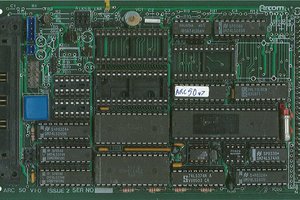
Uses the MC146818 RTC and opto-isolators to isolate RAM control signs when unpowered.

In the early 1980s, RAM was expensive and separate boards were an important way to expand memory. This board had up to 6 x 8 = 48 kilobyte of battery backed CMOS RAM. These days you can get a 512 kilobyte RAM chips very cheaply, so plenty of RAM can fit on a CPU board.

The MC146818 used to be a very common RTC in a DIP28 package. These days you can get an RTC in a DIP8 or smaller package, which can also fit on a CPU board.

The board uses opto-isolators to write-protect the RAM when the power is below the safe working minimum, but these days one would use a write-protection circuit from Dallas Semiconductors.

J058_SCRAM_manual.zip

Board manual with circuit diagram and Motorola MC146818 datasheet.

Zip Archive - 9.85 MB - 05/05/2024 at 00:29

Download

  • PCB tracks

    Keith10/21/2024 at 19:30 0 comments

    I thought I had one or two of these boards but could not find any in my box of STEbus boards. They may be elsewhere but I can't find them right now. :-(

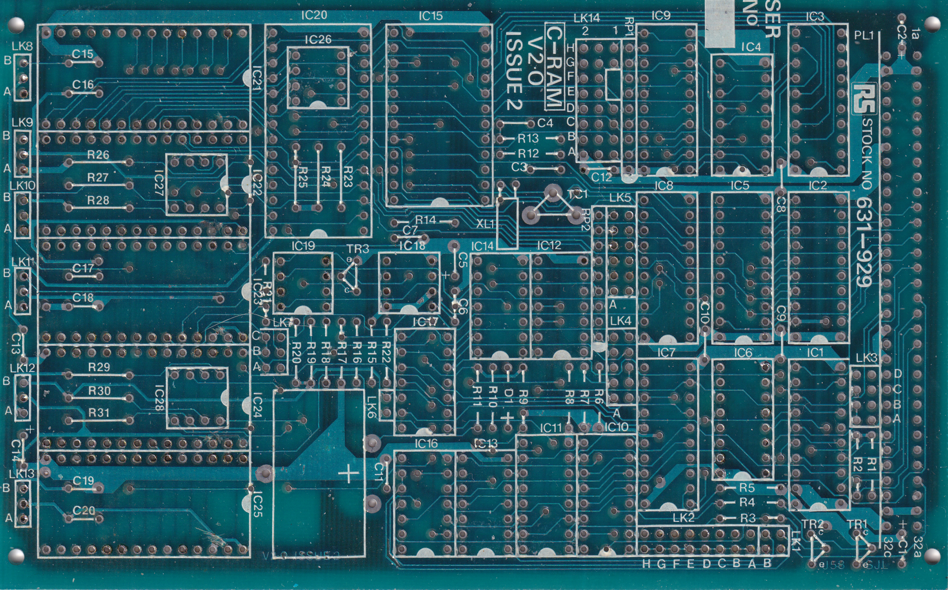
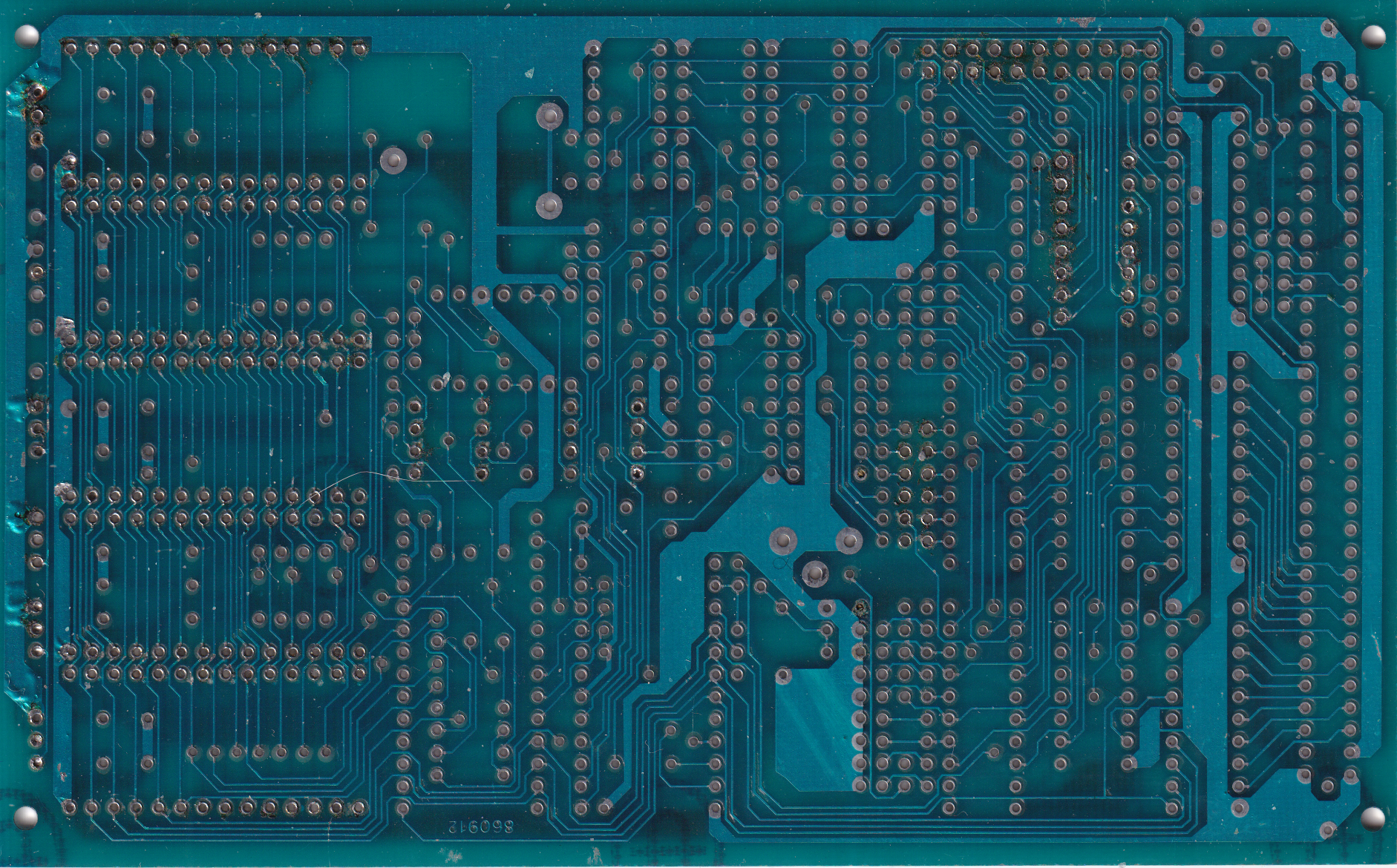
    I did have a bare PCB of the version 2 issue 2 board, with the PCB legend modified as requested by RS Components.

    Top

    Bottom

    If I don't have a complete board it means I don't have the PAL equations either. However, this is a fairly simple board so I doubt it would be hard to create PAL equations for it.

  • Catalogue page

    Keith05/02/2024 at 18:41 0 comments

    SCRAM

    A combination of battery-backed RAM and real-time clock is offered by the SCRAM board, providing STEbus systems with facilities for applications such as data logging or pseudo EPROM for software development.

    On-board are six 28-pin sockets which can be used for either 2k or 8k RAM or EPROM devices, allowing a total capacity of 48 kbytes. Jumpers provide great flexibility over where the RAM resides in the bus memory space, each of the six RAM sockets can be individually switched in or out of the selected block. You can select whether the card draws power from the bus or the on-board Ni-Cad battery. It is also possible to route the battery power onto the STEbus VSTBY line so that other cards can utilise it.

    The real-time clock facility is based on the HD 146818 chip, providing hours, minutes, seconds, day-of-week, data, month and year information, as well as an alarm for programmable or periodic interrupts. The chip also provides 50 bytes of RAM for storage of clock or other data in the event of power failure.

    Clock access is 1 microsecond. RAM access is under 400 nanoseconds.

    STE bus

    the board implements a simple slave interface to the bus; RAM can be located anywhere in the memory space; the realtime clock registers are mapped into the bus space, and can jumper-selected in 16, 32 or 64 byte blocks.

    Power Consumption

    typically under 0.5A at 5V when operating, and less than 200 µA when powered down.

    Features

    • six 28-pin memory sockets
    • up to 48 kbytes capacity
    • complete battery-backing
    • real-time clock with 50 bytes RAM
    • write protection on clock and RAMs

View all 2 project logs

Enjoy this project?

Share

Discussions

Similar Projects

Does this project spark your interest?

Become a member to follow this project and never miss any updates