 Yann Guidon / YGDES
I just came across this very recent measurement on the latest Intel 2xx series chiplet-based CPU. It's interesting because it gives a modern view of the best performances and latencies the bleeding edge can achieve.
See the source there:
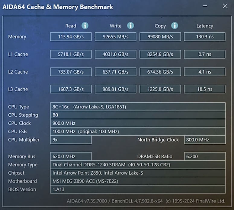
The main memory is still slow, hovering around 100ns, nothing new here. The quoted 130ns is from a misconfigured motherboard and an update brings it to a less sluggish 83ns, which has immediate effects on the performance. Further architectural enhancements can only come from the usual methods here : larger buses, more channels, more banks, tighter controller integration...
The interesting parts here are the latency ratios of the cache levels. L2=5.8×L1, L3=L2*5.6
Oh and that system can clock to 5.7GHz, so one L1 hit takes 4 clock cycles, and God knows how many instructions per cycle one such core can execute in this time.
An interesting outlier is this datapoint : L1 copy is faster than read or write. Some mechanism is at work here, probably "locality" or "streaming", with a large bundle/buffer that groups words and aligns them or something.
Note that 5.7GB/s at 5.7GHz amounts to one byte per cycle. That's decent but not much.
.......
The YGREC32 is not designed to work with the fastest silicon processes and most expensive foundries but the above numbers are rough estimates for the ratios that will be encountered in a "good enough" implementation. The point is that the architecture must be scalable and requires only little adjustment during shrinking.
This first thing we can conclude is that without L3 yet still following the "6× per level" rule-of-thumb, the CPU can't run much faster than one GHz or so. More or less, it's the L3 that enables the latest CPU to reach and keep running abot (say) 1.5GHz.
The other lesson is that memory latency is really, really important. An in-order CPU spends a lot of time waiting for data, leading to ever-increasing cache sizes and levels, as well as very deep out-of-order cores. Increasing the number of cores is another aspect, and Simultaneous MultiThreading helps with keeping the cores busy.
The worst problems come from OOO and the "solution" for this, explored in Y32, is to explicitly prefetch. The data are already playing the prefetch game since the D/A register pairs implicitly work like "reservation stations". Y32 has 16 such stations for data and 8 for code. This is comfortable maybe up to 500MHz or so. Faster clocks will require SMT, which is easy with Y32 but more than 2 threads will significantly bloat the core's area, so more cores become necessary.
OK, let's have two cores with 2× SMT for a decent speed. Now we hit two major walls: the FSB bandwidth wall gets hammered and there is probably not enough parellelism in the workload to occupy the cores. In interactive workloads, the separate cores act as local caches for the threads, since there is less space to move around, load to and spill from the caches. There is an incentive to keep as much data as possible onchip and swap only infrequently used data offchip. Speaking about swapping, this means that data blocks are more or less treated at the page level, or somesuch coarse granularity to increase efficiency, but this also increases latency by preventing multiplexing.
So overall, the clock range for Y32 would be from about 100 to 500MHz without extra architectural features. Out of the box, it could handle up to 16+8+2 concurrent memory transactions (data, instructions and stack) per thread. That's good but can only be exploited by good code, made by good compilers that can think beyond the old load-store paradigm.
The limiting factor will be the number of "reservation stations" (D/A registers and eBTB entries). FC1 will double them but that might not be sufficient, yet there is only so much space in an instruction word. "Register windows" and remapping of addressable resources will become necessary to push beyond the gigahertz hill.
Discussions
Become a Hackaday.io Member
Create an account to leave a comment. Already have an account? Log In.