TJ
TJ-
PCBs have arrived!
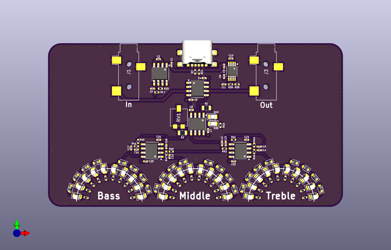
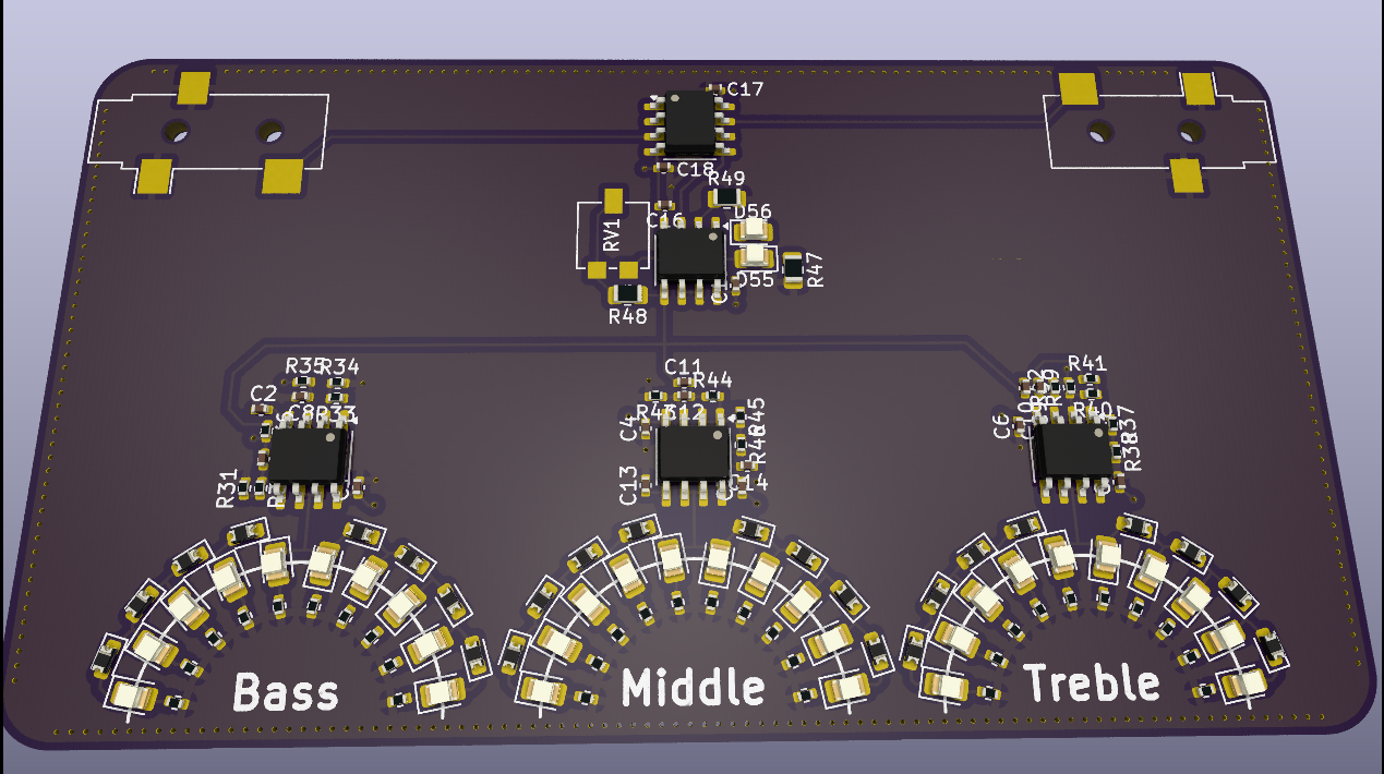
07/01/2024 at 16:54 • 0 commentsThe PCBs came in on Friday, June 28th and they looks pretty good. Below is a picture that includes almost completed boards and some boards still on the panel.
![]()
The matte black soldermask was a good choice. I made a mistake that wasn't caught until assembly and I opted for the manufacturer to send the parts with the PCBs and I would finish the assembly. The USB C part, in the BoM, had the THT tangs for the shield and the footprint used was for an all SMD part. This is easily fixed by bending the tangs out.Now the part that you've all been waiting for. Does it work? No. After doing some preliminary testing. I have a few ideas where the flaws in the design lay.
The video below shows a bit of testing. Had to bypass the USB C connector to supply power to the board. I also used a Analog Discovery 2 as a waveform generator to inject a triangle wave to see if the LEDs would sweep across the VU meter ark.
1. In testing, the +/-2.5 volt regulators were working as designed. This was confirmed with testing the voltage rails of each op-amp. Now the problem with the +/-2.5V rail design was that it was flying too close to the Vf of some of the LEDs. The next revision will use +/-5V regulators to widen the power rails.
2. The mids filter did not work at all. Troubleshooting signals was difficult due to the size of the components used in the filters. To rectify this, the new design will use larger components and incorporate some test points to make probing signals easier.
It is disappointing that the design did not work with the first go. But let this serve as an example that a design might not work on the first go and that a few revisions may be needed to realize the idea behind the project.
-
Updated BoM
05/26/2024 at 19:52 • 0 commentsUpdated the BoM after finding a discrepancy with the manufacturer part number and the footprint.
-
Day 14 (05/20/2024)
05/21/2024 at 02:12 • 0 commentsAdded contact info, revision number, and project name onto the front silkscreen.
![]()
Started the quote process to get some boards fabricated.
Started to setup the project on hackaday.io
-
Day 13 (05/19/2024)
05/21/2024 at 02:06 • 0 commentsNo work was done this day.
-
Day 12 (05/18/2024)
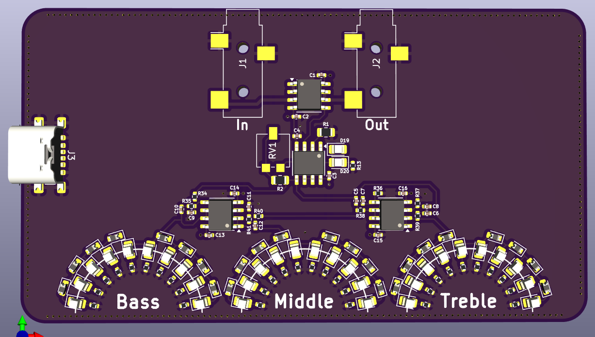
05/21/2024 at 02:05 • 0 commentsThe component reduction revolved around the band pass filter. Removed that LM358 and used the extra op-amps from the bass and treble sections.
![]()
After getting the schematic staightend out. Worked on re-laying out the filter sections. I'm a bit happier with the layout of the filter section. It's kinda starting to look like a dude at a turn table or that one boss from FF7.
![]()
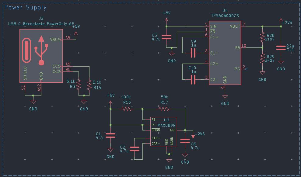
Designed the power supply circuit around the MAX889R and the TPS60500 for the dual rails. Both are capacitor based switching regulators. The input power is coming in from a USB C PD connector.
![]()
Laid out the USB C connector and the regulators toward the top center. This really makes the circuit look like Air Buster from FF7.
![]()
-
Day 11 (05/17/2024)
05/21/2024 at 01:58 • 0 commentsStarted to layout the filters, input/output buffers, and the amplifier components. Wasn't too happy with the layout. Then I had an epiphany to reduce the number of components. But that will have to wait until the next day.
![]()
-
Day 10 (05/16/2024)
05/21/2024 at 01:57 • 0 commentsNo work was done on this day.
-
Day 9 (05/15/02024)
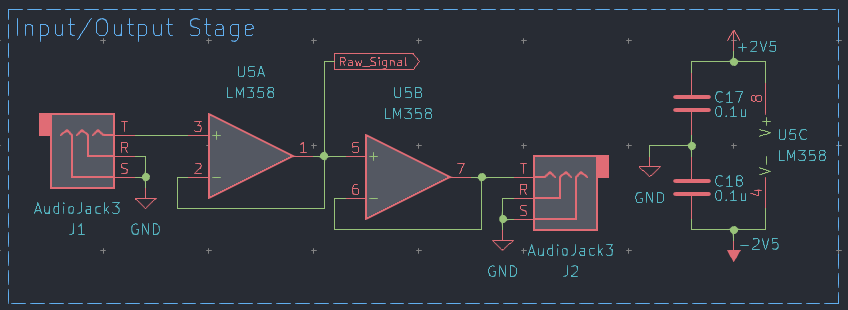
05/21/2024 at 01:57 • 0 commentsThe input and output buffer once again uses the LM358. I went with two 3.5mm jacks, since 1/4" jacks probably would make it hard to put the business card in a wallet. The final section to design is the power supply.
![]()
-
Day 8 (05/14/2024)
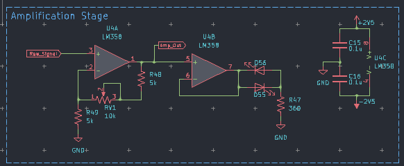
05/21/2024 at 01:54 • 0 commentsWorked on getting the amplification stage done after a brief stab at getting the correct spice models working in LTSpice and NGSpice. I will pursue getting the LM358 spice model working after I complete the rest of the circuit.
The amplification stage is using half of an LM358 in a non-inverting configuration to give a minimum gain of 4.125 V/V and a max of 10.375 V/V. I may change the values if I have to increase the rail voltages.
The other half of the LM358 is being used a indicator to make sure that the signal is being amplified before it makes its way to the filter stages.The next part that I work on is going to be the input and output buffers. I'll leave that design a surprise.
![]()
-
Day 7 (05/13/2024)
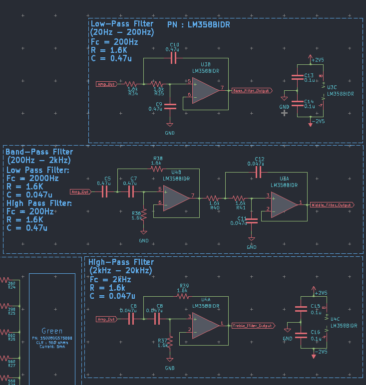
05/21/2024 at 01:54 • 0 commentsFilter Design
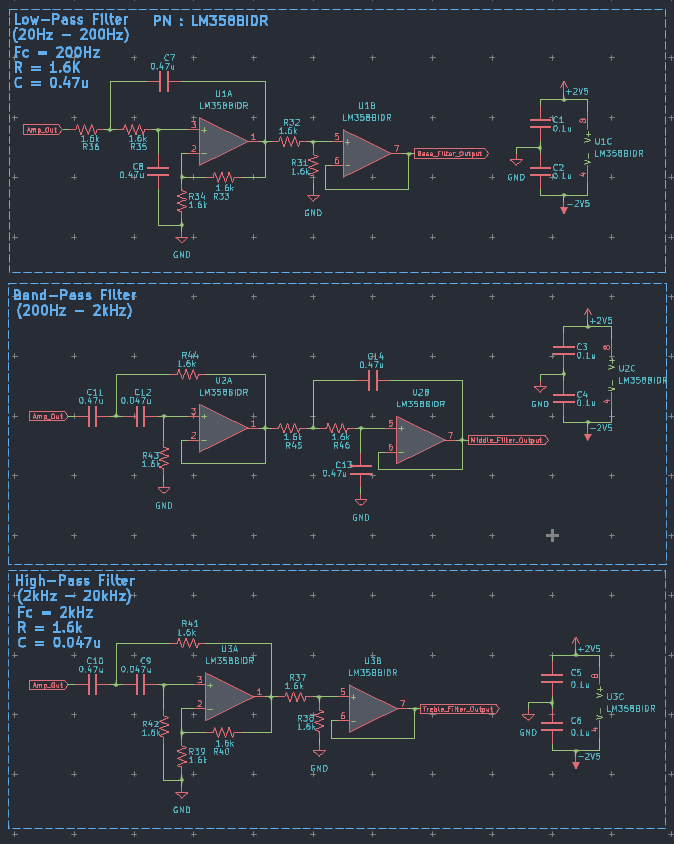
Each of the filters for the VU meters are 2nd order Sallen-Key filters. The op-amp of choice is the LM358B. The LM358B has the ability to run off a split rail and the output current should be enough for the LED arrays. The low-pass and high-pass filters were desgined first to get the values for the caps and resistors for the specific cutoff frequencies. This allowed the band-pass filter to be assembled from both filters. Side note, no testing/simulations of these filters have been done. We are flying by the seat of our pants here. I tried utilizing each op-amp in each package. This might not be the case with the actual amplification stage. A personal goal is to keep the BoM small.
![]()