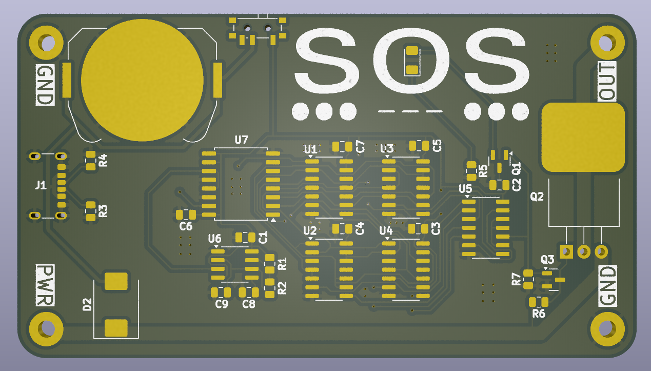
PCB designed using KiCAD. I tried to use SMD as much as possible, for ICs - SOIC package and for discrete components - 0805 size package.
Check schematics.pdf for full circuit schematics. There are some custom symbols and footprints used in this project. Those can be imported from this github repository.
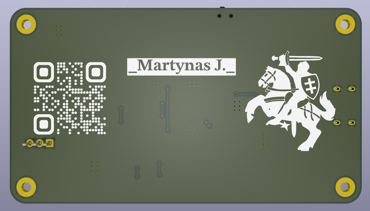
PCB is dual sided with most of the traces on top layer. Bottom layer dedicated for business card stuff - name, barcode which points to my github and artwork.
I ordered PCB on JLCPCB with black soldermask and board thickness of 1.2 mm.


 Martynas
Discussions
Become a Hackaday.io Member
Create an account to leave a comment. Already have an account? Log In.