 cheetah_henry
Finished the PCB design. The 3D rendering looks good. Sent to PCBWay for fabrication today. The Kicad design files are now available at my GitHub.
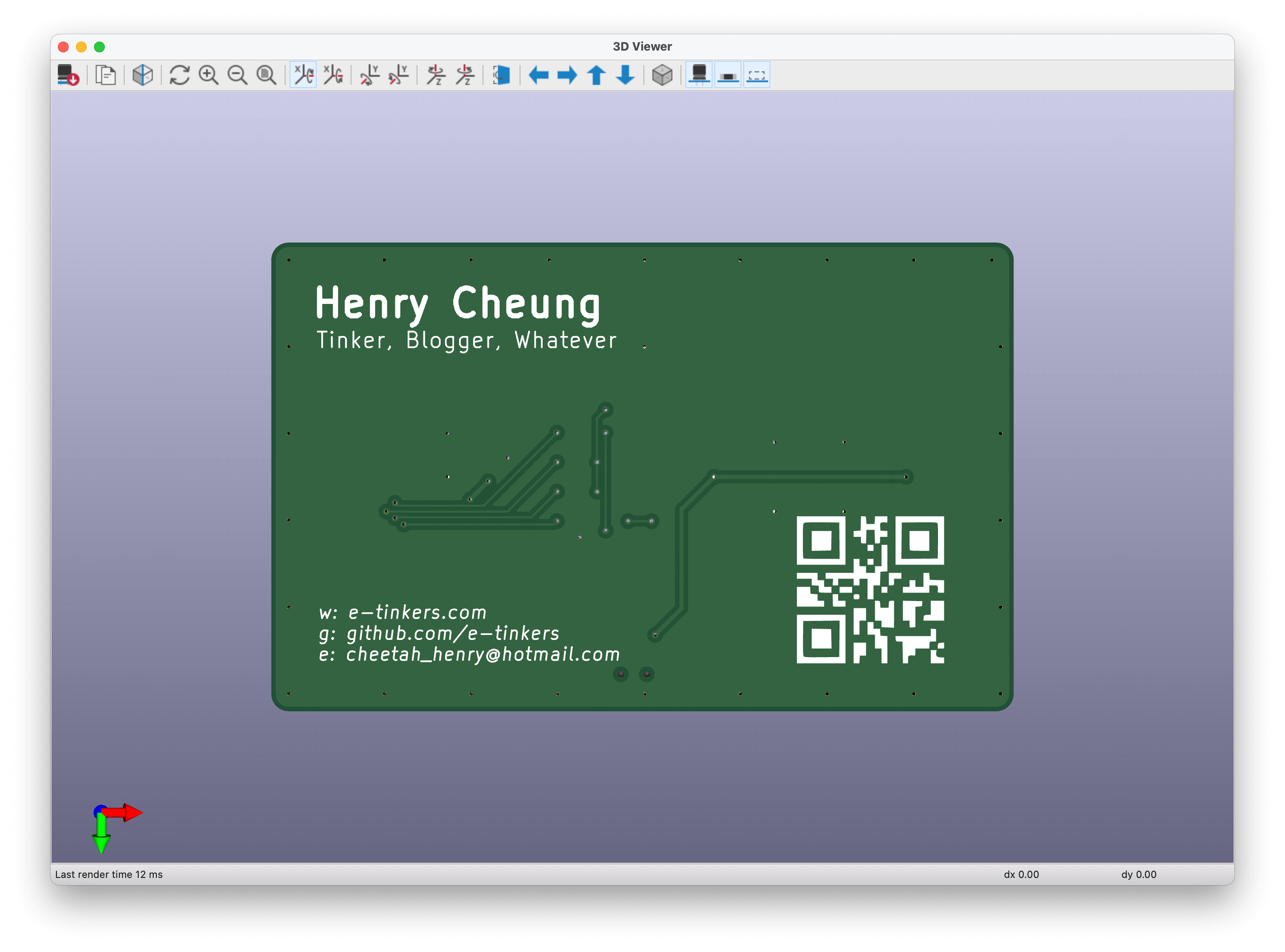
PCB 3D render (Name Card side)
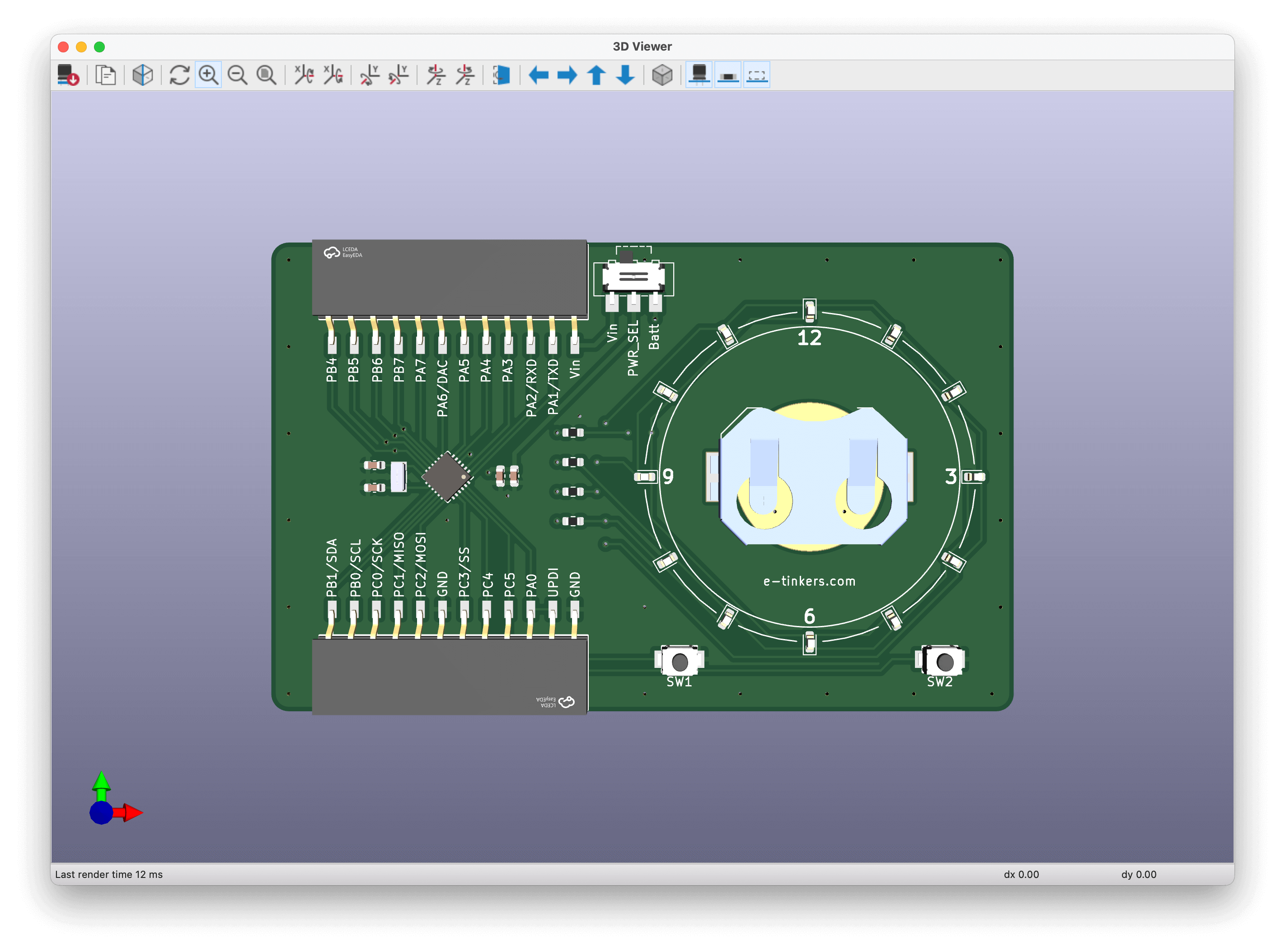
PCB 3D render (Component side)
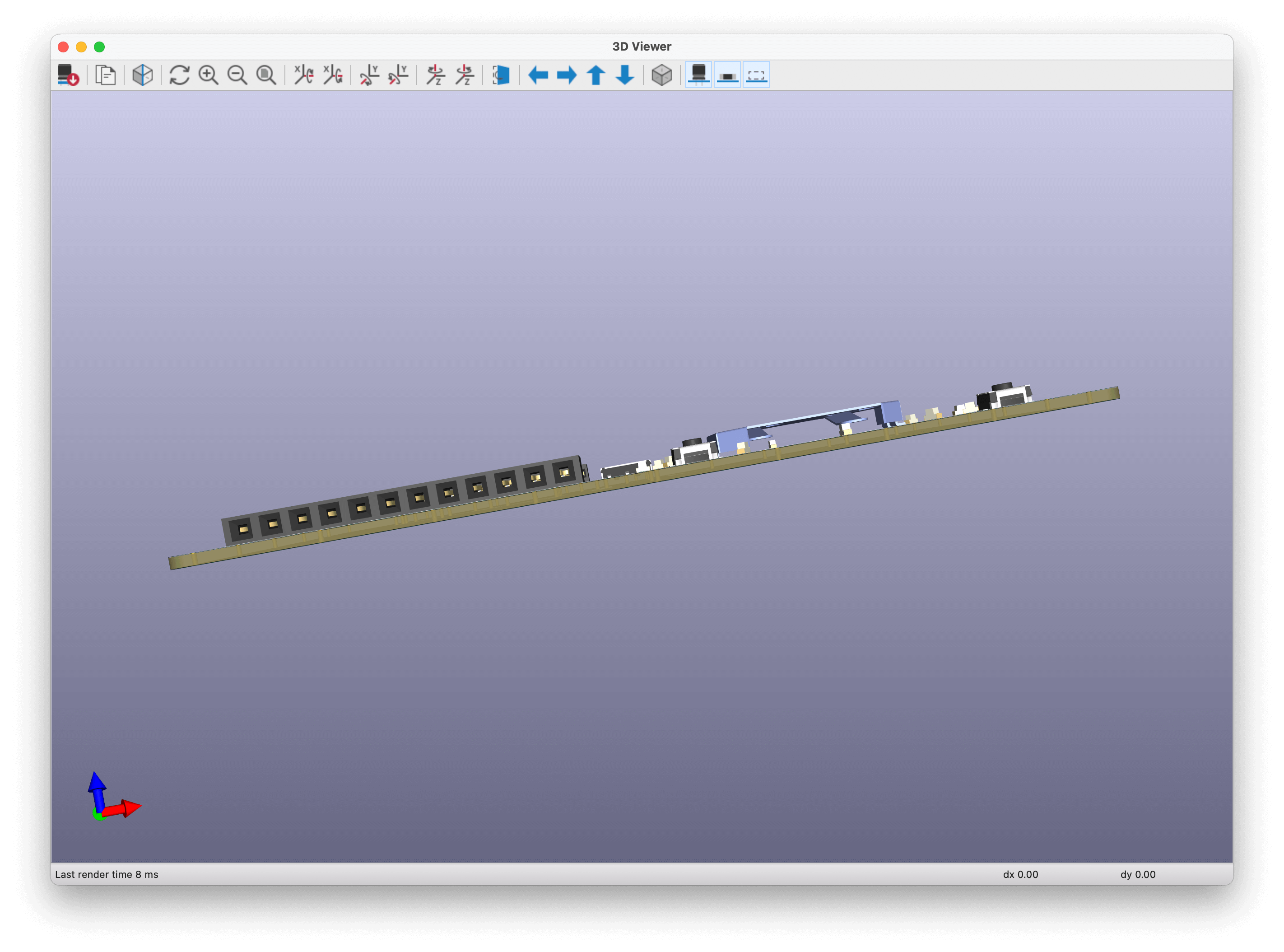
PCB 3D render (Thickness 3.2mm in total)
A project log for Business Card + Clock + ATtiny3227 Dev Board
A business card with a charlieplexed realtime clock and an ATtiny3227 development board.
Finished the PCB design. The 3D rendering looks good. Sent to PCBWay for fabrication today. The Kicad design files are now available at my GitHub.
PCB 3D render (Name Card side)
PCB 3D render (Component side)
PCB 3D render (Thickness 3.2mm in total)
Discussions
Become a Hackaday.io Member
Create an account to leave a comment. Already have an account? Log In.