-
Afterthoughts…
02/06/2017 at 08:57 • 0 commentsWith the testing of the AVR Data Recorder completed and a few sample test runs, I was fairly satisfied with the performance and features I was able to pack into this little device. The flexibility, hardware support and program-ability of using AttoBASIC as the underlying “operating system” allowed me a level of features that I have not seen in other data recorders on the market.
In using the AVR Data Recorder, I found that there were two features that I wanted to add.
- Low battery detector
- Temperature and humidity measurement
Low Battery Detector: In hindsight, I realized that I had not included a means to measure battery level, report and act upon a low battery condition. The AVR series of micro-controllers supports a “brown out detector” but all it really does is set a flag in the MCU status register that a power supply voltage less that a preset value occurred. The AVR can then respond to that condition. However, in the case of the AVR Data Recorder, there wasn’t much I could do since AttoBASIC does not process nor respond to “brown out” conditions. I also did not have any extra analog channels (nor pins) available to monitor the battery, which could easily have been accomplished using AttoBASIC. I began looking for an external “low-battery” detector circuit. I found a few designs in applications notes from MICROCHIP, LINEAR TECH and TEXAS INSTRUMENTS using their very-low power op-amps but in investigating their actual run current, I found that they would just add to the battery drain more than I wanted.
Not being satisfied with those solutions, I decided to investigate the power requirements of using an 8-pin TinyAVR. I had a tube of ATtiny13A’s available as well as some ATtiny25’s, 45’s, and 85’s but those would be an overkill in terms of available FLASH memory. The ATtiny13 looked like the right choice. It has an internal 1.2 MHz oscillator, an ADC and a few I/O pins. It would have to run off the 3 volt supply of the AVR Data Recorder but the Li-Ion cell could attain a charged voltage of 4.2 volts, too high for a direct ADC input. A simple solution was to add a resistor network voltage divider before the ADC pin but I wanted to conserve power and using the ADC would use extra power. The analog comparator uses very little power, so it was a good choice. I figured I could set a threshold for the analog comparator “AIN1” reference input by using one of the PWM channels to create a “poor-man’s” DAC, which requires only a resistor and capacitor and the original voltage divider method works with the analog comparator as well. Using the PWM to set the reference voltage allowed me to implement a sort-of hysteresis along with a voltage averaging to minimize variation in the battery voltage readings.
To warn the user that the battery is low, I decided to add an LED that I could “blink” every few seconds. In testing, I settled on a 64 mS “blink” time and a low-current red LED.
Like all AVR’s the ATtiny13A could enter a low-power sleep mode and I could use the watch-dog timer to wake it with a “system reset” every 8 seconds, which is the longest timeout available for the watch-dog timer. Essentially, I would just run through the program sequentially from RESET to END with each timed “wake-up”.
The program sequence is as follows:
1 RESET
2 load preset AComp reference value
3 set I/O ports
4 set PWM to reference voltage
5 wait for PWM to settle
6 check analog comp
7 if low-battery detected
   a) set LED on
   b) set WDT for IRQ @ 64ms
   c) sleep till WDT IRQ
   d) set LED off
8 reset I/O ports
9 sleep in “power-down” till WD reset
The power consumption measurements were as such:
- AVR in powerdown = 4 uA
- AVR executing code for 64ms (setup and measure) = 160 uA
- AVR + LED “on” for 64ms = 1300 uA
The average power consumption = 125 uA with LED on, 42 uA with the LED off. It
beat the micro-power comparator in half as many parts!Below, in the photo on the left is the Low-battery detector installed in the AVR Data Recorder. On the right is the component locator of the Low-battery detector.
![AVR Data Recorder - added low-battery detector]() AVR Data Recorder – added low-battery detectorLow-battery detector – component locator
AVR Data Recorder – added low-battery detectorLow-battery detector – component locatorThe AVR Low-battery detector was a separate project but it was inspired for the need on the AVR Data Recorder. I may create a separate project log for it at a later date.
Temperature and Humidity measurement: One day, I found I had a need to monitor temperature and humidity conditions at a storage location that I had been using. Not having any means to capture and log temperature and humidity changes spurred an addition to the current design. I had already been working with the DHT-22 series of temperature and humidity sensors, even added support for them into AttoBASIC but my AVR Data Recorderlacked that feature. All I needed was one free I/O port, which I didn’t seem to have. In the original design, I had planned to use the ATmega328P’s internal 8 MHz oscillator BUT in case I needed lower power and a more accurate timing frequency, I designed in a 4 MHz crystal oscillator using two extra 74HC04 inverters. It’s output directly fed the ATmega328P’s X1 input through a jumper. I decided that I would use the X1 pin as an I/O port for the DHT-22. There was enough room on the back panel to add it and the plastic was soft enough to cut with a carpet knife and so the DHT-22 was added.
![20170124_084447]() AVR Data Recorder – main PCB
AVR Data Recorder – main PCBThe photo to the right shows the DHT-22 set into the left side (upper-left in the photo) of the back panel.
I charged the AVR Data Recorder and took it over to the storage location to leave for a week’s time. In my power calculations, I estimated at least 14 days of recording capability but figured that the “data file” would be filled long before then. I wrote the simple AttoBASIC program to capture and log the RTC time-stamp, integer temperature and humidity. I then retrieved the AVR Data Recorder and the data from it then created a spreadsheet to plot my data. I also added the daily high and low temperature readings to the data so I could see if the storage unit was truly “climate controlled” as I was paying extra for that feature. The resulting graph is shown below.
![storagebay_th]()
As can be seen, the temperature remains fairly consistent around 78° F but the humidity fluctuates between 71 and 84% RH. Being that the temperature in the facility seems to be set at 78° F, it is not possible to remove the excess moisture from the environment, so I would not necessarily consider the storage facility to be “climate controlled” because the excess moisture in the air causes the most damage in a closed environment, not to mention that it tends to encourage mold and mildew growth. If I am not mistaken, I believe that in order to maintain a low humidity environment, the temperature needs to be at least 75° F. Having the data in hand to support my complaint, I contacted the facility manager but she refused to adjust the temperature in the facility to 75° F or even 76° F saying that “it would cost too much in electricity“. As is typical with businesses, they tend to cut costs by providing only enough of a “feature” to justify the extra expense of said “feature”.
The AttoBASIC program used to capture and log the RTC time-stamp, integer temperature and humidity is shown below.
5 EMI $0C                        # CLEAR SCREEN
10 DFV 0; DFI 0 255; DFX         # CLEAR ALL PAGES OF DATA FILE
15 RTI 2                         # SET 100MS RTC INTERVALS
20 DHU 0; DHS 0                  # SET DHT READING PARAMETERS
25 RTR                           # RESET RTC TO ZERO
30 DHT                           # TAKE A DHT READING
35 A:=PEEK $5 $69                # FETCH THE DATA FILE HIGH POINTER
40 B:=PEEK $5 $68                # FETCH THE DATA FILE LOW POINTER
45 M:= A= $FF; N:= B> $FE        # TRICK TEST FOR ADDR=0XFFFE
50 IF M & N THEN GOTO 125        # IF LAST ADDRESS, EXIT
55 DFL PEEK $5 $63               # FETCH RTC BYTES (ALL FOUR)
60 DFL PEEK $5 $64
65 DFL PEEK $5 $65
70 DFL PEEK $5 $6A
75 DFL PEEK $5 $6C               # FETCH DHT INTEGER TEMPERATURE
80 DFL PEEK $5 $6D               # FETCH DHT INTEGER HUMIDITY
85 PRI "RTP: "; RTP              # EMIT A USER MESSAGE
90 PRINT "*F : "; PRINT PEEK $5 $6C  # EMIT A USER MESSAGE
95 PRINT "%RH: "; PRINT PEEK $5 $6A  # EMIT A USER MESSAGE
100 PRINT "===============~"     # EMIT A USER MESSAGE
105 FOR N= 1 75                  # SET UP LOOP FOR 5 MIN DELAY
110 SLP 8                        # WAIT 4 SECONDS (75 * 4 = 300)
115 NEXT                         # END LOOP
120 GOTO 30                      # LOOP TILL DATA FILE IS FULL
125 DFF 6                        # SET FORMAT TO 6 BYTES/RECORD
130 END                          # END
Note that the “SLP 8” instruction reduces power consumption by the ATmega328P by placing it into the “idle state” and uses the internal watch-dog timer as the “wake” interrupt source.
Additional observation: Also in hindsight, I should have used the ATmega32U4. I have been using this part in another project for a few years. It has a built-in USB interface, a “bipolar” ADC and a few extra I/O pins.
This entry completes the project log for the AVR Data Recorder.
Peace and blessings.
-
Initial testing the hardware
02/06/2017 at 08:54 • 0 commentsOnce the PCB’s arrived and were assembled, I set out to test the individual components on the AVR Data Recorder. Once again, AttoBASIC was indispensable for this purpose. As of this post, the newest version of AttoBASIC (V2.34) is now available and adds support for several more AVR’s, including the ATtiny84 and ATtiny85.
Testing was easy and all the functional blocks worked as expected. I had to build a separate precision 1.000 volt reference to calibrate the analog front end but that was a fairly easy project.
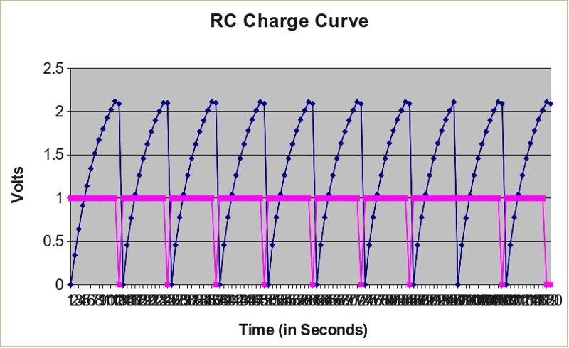
One of the tests I ran was using the digital output to short a large capacitor then using the analog comparator with the Vref set to 66% of the charge voltage, wait for the charging voltage to reach the analog comparator’s trigger threshold. The data was stored in the “data file” (off-chip EEPROM), later retrieved and imported into a spreadsheet so the data could be graphed.
The program used is shown below:
5 EMI $0C #CLEAR SCREEN
10 DFI 0 8; DFF 2; DFX # INIT 8 PAGES, 2 FIELDS PER RECORD, RESET ADRESS POINTER
15 DIG 1; ADG 0 2      # INSURE CAP IS SHORTED AND SET CH 0 GAIN TO 1X
20 R:= 16              # 2V ACO REF (0.1X ON ACO)
25 ACR R; SLP 5        # SET ACO REF AND DELAY 500MS
30 PRINT "TESTING ACO TRIGGER LEVEL...~"
35 FOR N= 1 10         # LOOP TEST 10 TIMES
40 PRINT "RUNNING TEST   # "; PRINT N; PRINT "~" # PRINT TEST #
45 DFL ADC 0; DFL ACO
50 DIG 0               # RELEASE CLAMP ON CAPACITOR
55 SLP 5; DFL ADC 0; DFL ACO   # SLEEP 500MS, TAKE AND STORE READING
60 PRINT "SAMPLING ...~"
65 IF ACO = 0 THE
70 GOTO 55                   # KEEP TAKING READINGS TILL ACO TRIGGERED
75 PRI "~ACO TRIGGERED AT "; PRI ADC 0        # PRINT THE VALUE
80 DIG 1                                      # CLAMP THE CAPACITOR
85 NEXT
The image below is the resulting data is presented as a charge voltage vs. time graph. The magenta line shows the state of the digital output, which was used to discharge the capacitor. The blue line shows the charge and discharge voltage across the capacitor.
![aco_dig_test]() Analog Comparator Test
Analog Comparator TestThe following program shows a typical usage for recording the 32-bit RTC value and all four channels of the ADC; Analog Channel 0, Analog Channel 1, TRMS Channel and the current reading channel. The RTC value is used as a “time-stamp”. Once the data is captured, it can be dumped from the AVR Data Recorder’s “data file” and imported into a spreadsheet for analysis.
5 DFI 0 1 ; DFX # init the 1st page as we need only 80 bytes and reset pointer
10 RTI 2; RTR   # set to 100mS update interval and reset RTC count
15 FOR N=1 10   # contain to 10 iterations
20 PRINT "N= "; PRINT N; RTP            # optional - print RTC on console
25 A:=PEEK $5 $65; B:=PEEK $5 $64   # RTC registers at 0x0562 {MSB} to 0x0565 {LSB}
30 C:=PEEK $5 $63; D:=PEEK $5 $62   # "$" means hexadecimal value follows
35 DFL D; DFL C; DFL B; DFL A       # log all 32 bits to data file MSB to LSB
40 DFL ADC 0; DFL ADC 1             # log Ch 0, 1 to data file
45 DFL ADC 2; DFL ADC 3      # log TRMS and Current sense to data file
50 FOR T=1 30                # SET UP 30 SECOND WAIT PERIOD
55 SLP 6                     # SLEEP FOR 1 SECOND
60 NEXT T                    # CONTINUE LOOPING
65 NEXT                           # loop to sample and record
70 DFF 8                    # set data format to 8 fields per record
75 # once finished, use "DFD 0 1" to capture the data
I later went on to monitor the dwelling’s water heater usage. It was a modified form of the above program. I had to design a Rogowski Coil and a front-end circuit to measure the water heater’s A/C current. I documented the construction technique in a PDF file here.
The image below shows the water heater “on” time over a 7 day period. Though, the actual time is difficult to see in the graph.
![waterheater_test]()
I spent a considerable amount of time creating a user manual and application note for this project. It contains information on the use of the AVR Data Recorder, specifications and programming techniques. The PDF file is here.
-
Designing the front and back panels for the enclosure
02/06/2017 at 08:53 • 0 commentsWith the PCB’s on order and the mechanical dimensions taken, I was able to start on laying out the front and back panels for my design.
I used an old version of AutoCAD, which I had learned back in the mid-80’s. I don’t use it much these days but sometimes it comes in handy.
The original front panel was used and all I added were the holes for the “ON/OFF switch”, Channel 0 and Channel 1 inputs. The square hole was just the right size to fit a USB mini-B plug through and was used to access the USB mini-B jack located right behind it on the PCB. Also present on the original front panel was a small whole, which had an LED behind it on the original device’s PCB. I used that as well by placing an LED behind it.
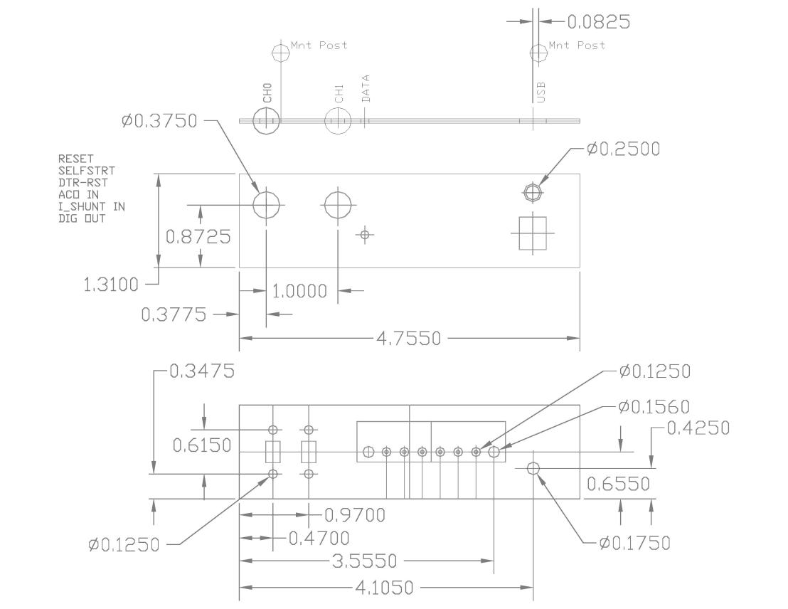
The back panel was cut from a larger sheet of plastic that I had acquired at the local “surplus electronics” store. It was a soft plastic that had a smooth side and an “orange peel” side. It took no effort to drill the holes using my drill press and the 1:1 alignment guides I printed. Below is the JPEG image of the front and back panels after I decided what mechanical components to put where.
![_faceplate]()
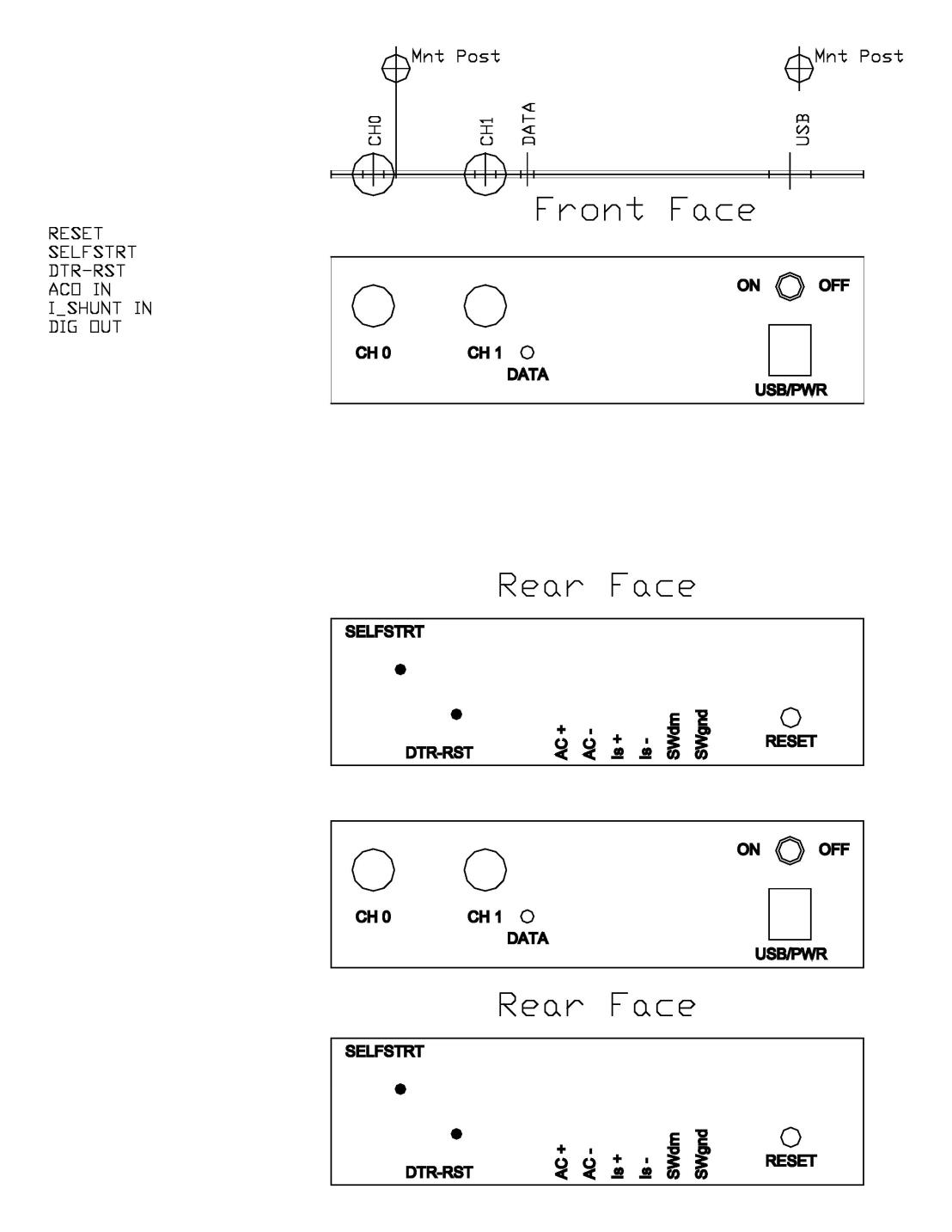
I also used the annotated 1:1 drawing printed on a full-sheet label, which I applied to each of the faces once the holes were drilled. This made a nice legend for each of the two panels.
Since the AVR is using OptiBoot (part of the ARDUINO IDE support files) for it’s boot-loader, I added a switch to enable switching in and out the DTR signal from the USB-to-Serial bridge. The DTR signal is used to pulse the RESET line of the AVR to initiate the boot-loader for programming. However, in debugging, the ATmega328P uses ATMEL’s DEBUG-WIRE® protocol and having the DTR signal connected causes DEBUG-WIRE® not to function.
The 2nd switch is used to tell AttoBASIC, which the AVR Data Recorder is using as it’s “operating system”, whether or not to auto-load and run the 1st program saved in EEPROM. Using this method, the AVR Data Recorder can be used as a “stand-alone” device or in “interactive mode”.
Below is the JPEG image of the legend text.
![_faceplate_text]()
-
Designing the PCB
02/06/2017 at 08:48 • 0 commentsWith all the features I could think to add into the AVR Data Recorder and having taken the available PCB dimensions, it was time to set out laying out the PCB. I won’t spend a lot of time on this subject but suffice it to say, I ordered 5 PCB’s from PCB Fab Express (http://pcbfabexpress.com).
WORDPRESS does not allow TXT and ZIP file uploads, so in my opinion, WORDPRESS is great if you are posting multimedia content but inflexible when it comes to posting project files. Thus, I have set up a PUBLIC link to the ZIP file with the GERBER files here. JPEG images of the GERBER layers are below.
![_datarecorderv100_gerber-1]()
Once the PCB’s arrived, they assembled without any issues.
-
Hardware Features
02/06/2017 at 08:47 • 0 commentsWhile thinking about the features I wanted for my AVR Data Recorder, since it will be AVR based, I wanted to use as many feature of the on-chip peripherals as possible, so I came up with a preliminary list;
- 2 analog channels with programmable gain and attenuation
- bipolar inputs
- true RMS reading for complex A/C waveforms
- a means to accurately measure current through a device
- an analog comparator to detect “events” to start and/or stop data capture
- a high-current digital output for switching loads, perhaps driven by a low-frequency source
- a means to record data and “time stamps” to EEPROM
- a means to replay or dump the captured data
- a means to “set and forget” with a single push-button to start the data capture
- run on a rechargeable power source
- programability
- nice plastic enclosure with a front and back panel
- above all, use components that I already have in stock
To that avail, here are the parts I selected to accomplish those hardware requirements:
Enclosure: I happened to run across some nice “used” plastic enclosures at the local surplus electronics store. Some of them had existing PCB’s in them, which meant that there was internal mounting posts for those PCB’s. Since this was intended to be a “one off” project, I settled on a nice plastic enclosure measuring 5 x 5 inches with a removable aluminum front and back panel. I could make use of the front panel but the back panel was not going to suit my purposes. I did however, have some soft plastic sheeting that I could easily and accurately cut with a utility knife. With an enclosure decided upon, I removed it’s PCB and took some dimensional measurements to determine how much PCB area I would have available for components and off-board connectors.
![AVR Data Recorder]() AVR Data RecorderAVR Data Recorder – front panelAVR Data Recorder – back panel
AVR Data RecorderAVR Data Recorder – front panelAVR Data Recorder – back panelThe enclosure is shown in the left photo above. I am getting a little ahead of my build here but the middle and right photos show the final front and back panels.
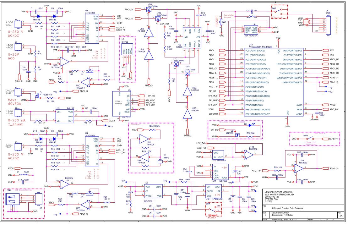
![_datarecorder_1v00a]() AVR Data Recorder Schematic V1.00A
AVR Data Recorder Schematic V1.00AThe above schematic is available as a PDF file here.
2 analog channels: The ATmega328P (U13) contains a 10-bit ADC and can sample 9 channels plus “ground” (0.0 volts), the internal 1.10 volt reference and the on-chip temperature sensor. I would only be using 2 of the analog channels for the variable-range analog inputs because adding more would mean adding more gain and attenuation circuitry. Note that although the two analog inputs are “bipolar”, the ATmega328P is not. Meaning that the ATmega328P can only measure voltages between o.0 and “Vref” volts. In hindsight, I would have been better to select the ATmega32U4 because it does support “bipolar inputs” and has a built-in USB hardware interface.
Programmable gain and attenuation: The AVR’s input range is limited to it’s (internal or external) Vref, which means it’s input range would be only 1.10 volts. To gain a broader range, I elected use a 2.50 volt reference to extend the range between 0 to 2.50 volts. 2.50 volts maximum on the input is just not enough, so I would need an input attenuation circuit to measure higher voltages and an input gain circuit to accurately measure voltages that could be under 0.5 volts.
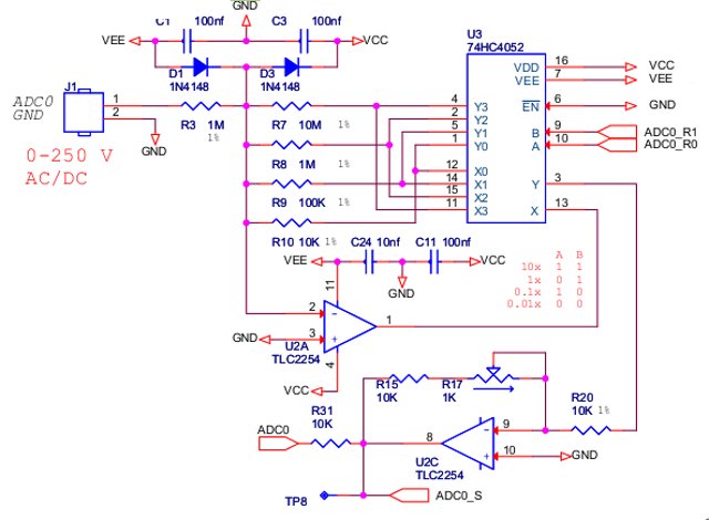
I already knew how to use operational amplifiers to create gain and attenuation circuits but what I needed was a way to program the gain. Decades ago, I had designed an ADA compliant PUBLIC telephone handset for the “hearing impaired”. In that circuit, I used a series of two MOSFET’s to switch different gain setting resistors (R7, R8, R9 and R10). I did not wish to use any discrete MOSFET’s if I could, so I decided to look into the 4000 series of CMOS logic. From what I recalled, there was the CD4066 and CD4052 analog switches, which I had used on other analog circuit designs years ago. I settled on the 74HC4052 (U3), which is a “Dual 4-channel Analog Multiplexer/Demultiplexer“. The typical “on resistance” at ±5 volts is 80Ω. In my calculations, the lowest resistor value in my gain circuit was 100 KΩ and had a 1% tolerance. 80Ω works out to be a 0.08% increase in the gain setting resistor, so at a 1% resistor tolerance, I did not see any need to be concerned as I was not designing a highly accurate piece of commercial or industrial equipment. Besides that, my measurements are limited to 8 bits with ±1 bits of conversion accuracy, which equates to less than 0.5% error, not including non-linearity errors.
The TEXAS INSTRUMENTS TLC2254A (U2A and U2C) used in the gain/attenuator circuit is an “Advanced LinCMOS RAIL-TO-RAIL VERY LOW-POWER QUAD OPERATIONAL AMPLIFIER” designed to be used as an analog front-end to Analog-to-Digital converters. The partial schematic below shows the gain and attenuation circuitry of one analog input channel.
![excerpt-analoginput]() Excerpt – 1 of 2 analog channels
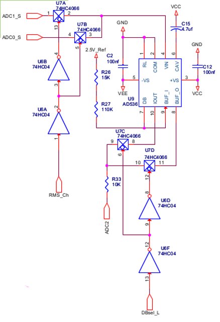
Excerpt – 1 of 2 analog channelsTrue RMS to DC conversion: I also had a handful of ANALOG DEVICES AD536A “True RMS to DC converters”. I thought it would be nice to add it so I could also measure complex waveforms, either true AC or AC on a DC bias. It will also work with a DC input, so that would get me the absolute value of the analog input. I decided to implement a means to measure the True-RMS on a separate ADC channel but allow a means to switch it between either of the two analog inputs. The AD536A has both DC and dBV outputs. Although theAVR Data Recorder can switch between either one, the dBV output needs amplification in order to be useful but I neglected to add a 2x amplifier on the output BUT the AVR can be switched to use it’s internal 1.1 volt reference instead of the external 2.50 volt reference but the accuracy has a ±10% accuracy. The internal reference’s long-term stability is not specified. The partial schematic below shows the AD536A (U9) using 74HC4066 (U7A/B/C/D) analog switches to select between the two analog channels (ADC0_S andADC1_S).
![excerpt-ad536a]() Excerpt – AD536A True RMS to DC
Excerpt – AD536A True RMS to DCCurrent measurement: I happened to also have some TEXAS INSTRUMENTS INA196 “Current Shunt Monitor” IC’s left-over from a previous project. I thought it would be great to have a means to measure current, which could be read on a separate AVR ADC channel. I did not wish to have too large a shunt resistor because it would increase the shunt voltage. I also did not have enough room on the PCB to add extra circuitry to switch in various shunt resistor values and since most of the circuitry I was using had operating currents under 200 ma, I decided to use a 0.5 Ω / 5 Watt shunt resistor, which would give me a measurement range up to 250 ma. The partial schematic below shows the implementation of the INA196 (U15) and the shunt resistor (R4).
![excerpt-currentshunt]() Excerpt – INA196 Current Shunt
Excerpt – INA196 Current ShuntAnalog comparator: The AVR has a built-in analog comparator. I thought this feature would be useful for detecting certain events and using them as a “trigger or halt the capture” mechanism. The input range would be limited to the supply rails of the AVR, which was 3 volts, so I thought it would be best to add a 10:1 voltage divider, yielding a 0 to 25 volt input range.
For the reference input, the AVR allows the selection of either an ADC channel or an external reference. I chose to allow access to both analog channels and create an adjustable reference voltage using one of the AVR’s PWM outputs filtered through a simple R/C network to derive a simple D/A converter. This way, I could set the reference input anywhere between 0 and 2.50 volts or translated by the 10:1 divider on the input, 0 to 25 volts. The partial schematic below shows the analog comparator input divider (R1/R2) on the left and the PWM R/C filter (R29/C23) and TLC2252 buffer (U14A) that creates the analog comparator’s reference voltage on the right.
![excerpt-analogcomp]() Excerpt – Analog Comparator and Reference
Excerpt – Analog Comparator and Reference![excerpt-vref]() Excerpt – ADC Voltage Reference
Excerpt – ADC Voltage Reference“External” ADC Voltage Reference: The ATmega328P has an internal 1.1 volt reference that can be used as the ADC reference. I wanted to have a full-scale reading of 2.50 volts, so I decided to use an external reference for that purpose. I chose to use a MAX6002 “Low-Cost, Low-Power, Low-Dropout, SOT23-3 Voltage Reference” as I have been using them on another project. The MAX6002 has a 1% accuracy and a long-term stavility of 50 ppm (over 1000 hours). The analog comparator’s PWM reference generator was using 1/2 of the TL2252, so I used the other 1/2 as a voltage follower to supply a voltage reference to the AD536A. The partial schematic on the right shows the implementation of the analog voltage reference using the MAX6002 (U10) and 1/2 TLC2252 (U14B).
![excerpt-digitaloutput]() Excerpt – High-current Digital Output Driver
Excerpt – High-current Digital Output DriverHigh-current digital output: In thinking about any extra features that I could stuff in to this project, and using every available I/O port and feature of the AVR I could come up with, I decided to add a means to switch a medium current load. I had a few higher-current MOSFET’s available in my sample stock but I wanted one that had a low Rds(on) and could handle at least 40 volts @ 1 amp. I found the NTF3055-175 (Q1) fit that role pretty well and so it was designed in. The NTF3055-175 has a 60 volt Vdss, a continuous Id of 2.0 A (@25°C), a maximum of 175 mΩRds(on) and maximum Vgs(th) of 2.0 volts, which works well for this application. It is configured as an open-drain output with the source connected to GND. Although technically, I should have used an opto-isolator to drive the MOSFET, I have not had any problems switching loads at 12 volts DC.
Because AttoBASIC supports both port level switching and DDS (direct digital synthesis) on the same I/O pin, I thought that the output could be used to either switch a load at frequencies between 1 Hz to 20 KHz or be switch on/off under program control, perhaps upon the detection of an event by the analog comparator. The partial schematic on the right shows the digital output circuit.
![excerpt-eeprom]() Excerpt – EEPROM
Excerpt – EEPROMData capture storage: I had recently added a means to interface with an external EEPROM as a “data file” to AttoBASIC. One of the reasons was for use in recording data, such as the AVR Data Recorder. The “data file” is an external 64KB EEPROM that uses the AVR’s SPI (Serial Peripheral Interface) bus to communicate through. I used a MICROCHIP 25AA512 (U5) because I had a few in my sample stock. The partial schematic to the right shows the simple interface.
![excerpt-dht22]() Excertp – DHT-22
Excertp – DHT-22Digital temperature and humidity: After I designed, built and tested the AVR Data Recorder, I started to work with the DHT-22 (U?) temperature and humidity module. I added support for it into AttoBASIC and later decided to add it into the AVR Data Recorder, so this was an afterthought. The partial schematic to the left shows the simple 3-wire interface of Vcc, GND and the bidirectional “data” pin. Sadly, the DHT-22 is not DALLAS 1-Wire® compatible and has it’s own protocol, thus all the decoding “work” is done within AttoBASIC.
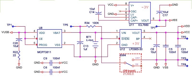
Support circuitry: The AVR Data Recorder was intended to run on a rechargeable Lithium-Ion battery source, specifically, the ICR18650NH type battery. These batteries carry a rating of 2200 mAh at a nominal voltage of 3.7 volts. I had salvaged quite a few of these batteries from DELL laptop battery packs that went bad. As is typical of laptop battery packs, usually only one or two cells actually go bad and the rest can be used. I decided that just one of these batteries would be sufficient for this project. I wanted to use a simple Li-Ion battery charger and MICROCHIP had a really simple one, the MCP73811 (U8) is packaged in a 5-pin SOT-23 housing and uses a single pin to set the charge current to either 85 mA or 450 mA. Since I would be using a USB interface to talk to the AVR Data Recorder, I could set the charging value to the higher 450 mA setting for charging from an external USB power supply or a computer’s USB interface.
Having only 3.7 volts (nominal) available from the battery, I chose to run everything off of 3 volts power supply. The LP2985-30 (U12) suited this purpose. The LP2985 series are “150-mA LOW-NOISE, LOW-DROPOUT REGULATOR WITH SHUTDOWN“. The suffix of “-30” means it is fixed to regulate at 3.0 volts. Although the LP2985 and MCP73811 run off the internal Li-Ion battery, I make use of the “shutdown” pin to power off the rest of the circuitry so the battery can be charged while plugged into a USB port or power-supply.
In designing the analog front-end for the two analog channels, I decided that it would be best to run all the analog components with a bipolar power supply of ±3 volts rather than a mid-rail reference running off of a uni-polar 3 volt power supply. Doing so would increase the accuracy and headroom of the analog front-end. The 74HC4052 (U3 and U4) needs a negative voltage when operating as an analog multiplexer, therefore it works well with the TL2254’s (U2) in the analog front-end. In order to obtain the bipolar power supply, I used the ICL7660 (a.k.a. MAX1040) “Switched-Capacitor Voltage Converters“. The ICL7660 is a REALLY old part and has been around for a very long time. If I am not mistaken, it was originally designed and sold by INTERSIL. The ICL7660 (U11) requires just two 10 uF capacitors, one as the “charge-pump capacitor” and the other as a”reservoir capacitor”. The schematic below shows the Li-Ion battery (BT1), MCP73811 (U8), LP2985-30 (U12) and ICL7660 (U11).
![excerpt-powersupply]() Excerpt – Power Supply
Excerpt – Power SupplyUSB to Serial Interface: The AVR has an on-chip hardware UART with a TTL-level interface. My laptop does not have an RS-232 interface, most these days do not. I chose to hard-wire in a prefabricated CP2102-based USB-to-serial bridge module for that purpose. Doing so allows me to supply power to the AVR Data Recorder directly from the USB power pins.
In the next posting, I will discuss more progress on this project.
Peace and blessings.
- 2 analog channels with programmable gain and attenuation
-
A Versatile AVR-based Data Recorder
02/06/2017 at 08:46 • 0 commentsOnce upon a time, I became interested in monitoring power usage of certain appliances and devices in my dwelling. In particular, the water heater and refrigerator. I wanted to be able to monitor their power consumption over a duration of time and knew I needed some sort of data recorder. I could purchase one but the better ones with 10 or 12 bit ADC accuracy were expensive. The lower priced ones seemed a bit underwhelming in feature as they were very basic. And yes, there were a few projects on “the net” at that time, even more nowadays. However, there was one thing they lacked and that was some sort of programmability.
Since I was very heavy into further enhancing AttoBASIC, I decided that it would be very easy to modify AttoBASIC by adding specific commands to support a data recording device. After all, I had recently added a real-time counter and “data recording to external EEPROM” features that would suit this project’s purpose very well.
What I came up with is the AVR Data Recorder, which is a versatile programmable device that can, among other things, be used to capture and store analog data for retrieval at a later date.
The programmability of this device is due to the AttoBASIC V2.xx interpreter with specific language extensions for use with the AVR Data Recorder. The interactive ability of AttoBASICmakes it easy to set up individual channel gain and attenuation levels, print measured ADC values when writing, debugging, data capture and recording programs.
![20170124_092924]() AVR Data Recorder
AVR Data RecorderAlthough this project was completed mid-August of 2012, I have decided to post it in a more accessible location. The project can be found hereon AVRfreaks.net as well. Note that AVRfreaksrequires a free account to access its content.
I will post a series of blog entries to document the design and fabrication starting with it’s features.
Features at a glance- Processing core is an ATMEL ATmega328p running at 8MHz.
- Versatile; can be used as a stand-alone data capture and recording device or connected to a USB serial console for real-time display and capture of data.
- Portable; Internal Li-Ion rechargeable battery runs up to 14 days on a single charge.
- Two (2) channels of analog input;
- 8-bit analog resolution (9.8 mV / bit @ 1x gain, post-attenuation).
- Each channel is bipolar (+/-) with respect to ground, reading is positive only.
- Software selectable input attenuation for a range of 2.5volts, 25 volts and 250 volts.
- Software selectable input amplifier extends sensitivity to 250 millivolts per channel.
- One (1) channel of True-RMS reading, software selectable between either analog channel (post-attenuation).
- Current sensing input with a range of 0 to 250ma, 0.5Ω series resistance, externally extensible.
- Analog comparator input;
- Comparator source is software selectable between dedicated input with fixed 0 to 25 volt input range or either analog channel (post-attenuation).
- 8-bit programmable reference.
- Digital output for control of external devices;
- Open-drain “low-side” N-MOSFET solid-state switch with 175 mΩ “on” resistance can switch up to 60 volt loads with 1.5 amps of continuous current.
- DDS (direct digital synthesis) for toggling at a specific frequency (1 Hz resolution, 1 Hz minimum frequency).
- Digital temperature and humidity sensor
- 64K bytes of internal data storage capability in non-volatile memory.
- Pre-programmed “out of the box” to record a 24-bit time stamp and both analog channels every 60 seconds for data recording up to 218 hours.
- “Data” LED indicates data file access.
- Programmable;
- Uses AttoBASIC programming language, a Tiny-BASIC with an enhanced hardware-orientated command set.
- Programs can be saved in internal non-volatile memory for execution.
- Switch-selectable “self-start” feature enables immediate user program execution upon power-up or an interactive (command prompt) mode for test, measurement and programming.
- Programmability creates a stand-alone intelligent capture device with decision-making and basic data manipulation capabilities.
- AttoBASIC features;
- User programmable using BASIC-like command syntax.
- 8-bit data handling with 26 variables.
- Arithmetic, logical and relational operators allow manipulation of data before storage.
- 32-bit Real-time counter for time-stamping of data in resolutions of 1 ms, 10 ms and 100 mS.
- Extensions to language for direct control of the internal hardware, including the on-chip analog-to-digital converter, gain settings for each analog channel, analog comparator, analog comparator’s DAC reference generator, MOSFET digital output and the internal non-volatile “data file” storage memory.
- Direct data file access allows data dump in ASCII text CSV format for importation into EXCEL™ and other data-processing applications. Number of data fields per record is user programmable from 1 to 255 fields.
- USB interface via Virtual Communications Port supported by all major operating systems (WINDOWS™, MAC OS-X™, and Linux).
- Internal boot-loader allows AttoBASIC updates or user-custom application software to be uploaded to the AVR’s internal FLASH memory.
 Scott
Scott

 AVR Data Recorder – main PCB
 Analog Comparator Test


 AVR Data Recorder Schematic V1.00A
 Excerpt – 1 of 2 analog channels
 Excerpt – AD536A True RMS to DC
 Excerpt – INA196 Current Shunt
 Excerpt – Analog Comparator and Reference
 Excerpt – ADC Voltage Reference
 Excerpt – High-current Digital Output Driver
 Excerpt – EEPROM
 Excertp – DHT-22
 Excerpt – Power Supply
 AVR Data Recorder