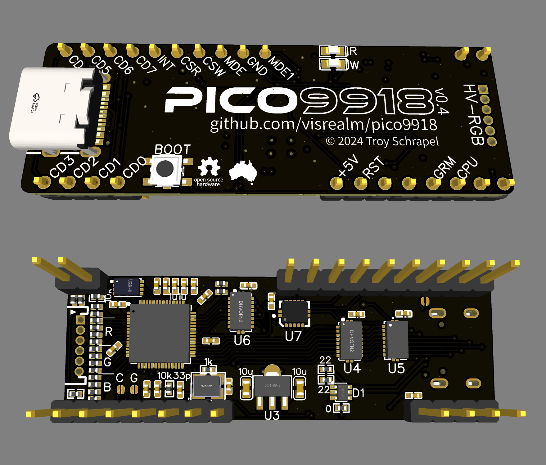
Started working on the next revision of the board (v0.4). The all-in-one.

Looking pretty good. Managed to have it mostly single-sided (good for cheaper PCBA). Most of the components will be on the underside. 4 layers with the middle layers being a solid ground pour and a (mostly) power layer. Signals mostly on the IC layer (bottom) with some on the back (top).
On the top side are a couple of optional LEDs for read and write (for those who like the blinkenlights). The Boot button and USB-C connector required for reprogramming to little RP2040.
Not ordering these yet as I like to give it a few days to "simmer" in case I think of anything I've missed or could do better. Likely order the initial batch next week.
 Troy Schrapel
Discussions
Become a Hackaday.io Member
Create an account to leave a comment. Already have an account? Log In.