PointyOintment
-
Introduction to GPUs and GPGPU
04/10/2017 at 05:21 • 0 commentsIt is time for the third type of processor I will be covering: the graphics processing unit (GPU). This is the one about which I know the least so far, so this will be the shortest post.
Specialized chips for graphics processing have existed since the 1970s. First used in arcade games, initially they served to connect the CPU to the monitor and provide graphics capabilities in a way that didn't require lots of RAM to store the image, or constant processing by the CPU to move 2D images around onscreen. In the late 1980s and 1990s, new devices were created that could handle basic 3D graphics calculations (transform, clipping, and lighting) in hardware. Again, the first of these were found in arcade machines. In 1996 and 1997 they became available in home video game and computer systems. Modern GPUs are descended from these.
Modern GPUs can perform programmable vertex shading and pixel shading. These consist of running a short program for each geometric vertex and each pixel in the output image. To speed this up, GPUs are built with many physical processing units (called shaders), which run these short programs (also called shaders) in parallel. Early modern GPUs' pixel shaders weren't actually fully programmable; they were more like blocks in an FPGA, programmable only for a certain set of functions. This was necessary to be able to run them at high pixel clock speeds to get all of the pixels in the image prepared in time. By the early 2000s, though, hardware pixel and vertex shaders were converging and also becoming more similar to CPUs, gaining looping and floating point math abilities, while keeping (and increasing) their parallelism. This soon came to be used for bump mapping, a process that simulates a texture on a rendered surface, even though the actual surface in the 3D model is flat.
Graphics APIs
Various APIs have been created to enable easy use of GPUs for graphics in your programs. They are useful for 3D games, 3D modeling programs, et cetera. OpenGL, a popular one, was first released in 1992 and is still used widely today. DirectX, a proprietary API (really a group of APIs, only some of which are GPU-related) from Microsoft, was first released in 1995 and is also very popular today, particularly for commercial games.
GPGPU
Most of the calculations used in 3D graphics are based on matrices and vectors, and involve doing a great many similar, simple calculations simultaneously, so modern GPUs are highly optimized for these demands. However, 3D graphics is far from the only field where highly parallel matrix and vector math is used. Using a GPU for non-graphics applications is called general-purpose computing on graphics processing units (GPGPU). This is done by means of compute kernels (or compute shaders), which are given to the GPU in place of vertex and pixel shaders. The data is usually provided in the form of a 2D grid, because GPUs are optimized for working with data in this form. Using a GPU to run a compute kernel on a grid of data is equivalent to using a CPU to loop over the grid and perform an operation during each iteration of the loop. However, the GPU performs the operation in parallel on multiple (perhaps all of the) elements in the grid simultaneously.
It is important to note that GPGPU is only effective for problems that can be solved efficiently by stream processing. While a GPU can solve problems where the subproblems are heavily interconnected, it will be much slower at that problem than a CPU, because the parallelism doesn't help with that type of problem.
When designing algorithms for GPGPU, you should try to maximize the arithmetic intensity (the number of arithmetic operations performed per unit of data), to keep the processing from being slowed down by memory access.
While you can do GPGPU using graphics APIs or direct access to the GPU, APIs also exist that allow easier use of GPUs for GPGPU, including OpenCL and OpenMP (both of which are not GPGPU-specific; they can run on many kinds of processors), as well as DirectCompute (part of DirectX).
GPGPU is useful for many scientific applications such as weather forecasting and climate research, bioinformatics, and astrophysics, as well as non-scientific (more immediately profitable) applications including audio, video, and still image processing, machine learning, data mining, cryptography/cryptanalysis, and computer-aided design and engineering. GPUs and GPGPU are commonly used in supercomputers.
-
Modern CPU Optimizations
03/20/2017 at 05:22 • 0 commentsComing soon…
I had planned to post this a month ago, but things got in the way. Watch this project log entry.
-
Introduction to Programmable Logic and FPGAs
03/20/2017 at 05:08 • 0 commentsAn alternative to serial processing such as is done by a CPU is programmable logic. In programmable logic, one defines a circuit of logic gates that achieves a desired result and programs this into a programmable logic device (PLD). Programmable logic devices include, in reverse order of invention and power:
- Field-programmable gate array (FPGA)
- Complex programmable logic device (CPLD)
- Generic array logic (GAL)
- Programmable array logic (PAL)
(The PLD type names all seem very similar and non-descriptive. I doubt anyone could tell which name corresponded to which architecture without being told.)
An FPGA is a device that, instead of having a (mostly) fixed circuit that performs computations according to a program, allows you to reconfigure its logic gates to form any circuit you want. It uses a different architecture than previous PLDs, specifically, using logic based on lookup tables (LUTs) instead of the pure gate-based logic used by the earlier PLDs. The "field-programmable" in the name simply means that it is programmable after leaving the factory, as opposed to a non-programmable logic chip, which is permanently configured at the time of manufacture.
FPGAs are used in many applications, including real-time processing, glue logic, and prototyping of application-specific integrated circuits (ASICs). Originally they competed in the glue logic market with CPLDs, but they soon grew into other markets as well, adding dedicated logic circuitry such as multipliers, which enabled their use for digital signal processing (DSP). Some modern FPGAs also have integrated CPUs and RAM.
Architecture
Logic blocks
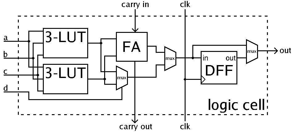
The base unit of the FPGA architecture is the logic block (aka configurable logic block, logic array block, logic element). This is a circuit that can be programmed to emulate any kind of Boolean logic gate. A diagram of a simple logic block is:
![]() Diagram by Petter.kallstrom, public domain
Diagram by Petter.kallstrom, public domainThe basic components of the logic block are two three-input LUT or a single four-input LUT, a full adder, and a D-type flip-flop. Between these components are multiplexers, which determine the routing of the signals through the logic block.
The left mux combines the two three-input LUTs into a four-input LUT. Some modern FPGAs have an actual four-input LUT instead.
The center mux is used to switch between normal mode and arithmetic mode. Normal mode means the output of the four-input LUT is passed to the right third of the circuit, while in arithmetic mode, the outputs of the 3-input LUTs are combined by the full adder and its result goes to the right third. (The full adder and the LUT-combining mux both always operate; the middle mux just chooses which of their outputs to use.)
The right mux is used to switch between the synchronous and asynchronous output modes. In synchronous mode, it takes the output of the D-type flip-flop, which passes on and holds its input signal upon receiving a clock pulse. In asynchronous mode, it takes the output from before the flip-flop, resulting in the output not waiting for the clock signal.
Together, all of these components can be programmed to emulate any Boolean logic gate. There may be hundreds to thousands of these logic blocks in an FPGA.
Hard blocks
Modern FPGAs also have hard blocks, which are dedicated logic circuits such as transceivers, multipliers, memories, and small CPUs. These are built in the normal way, as ASICs, instead of using logic blocks. This enables them to be much faster and more efficient, and leaves the logic blocks unoccupied for the user's circuits.
Routing
An FPGA also has switching components that connect the logic blocks to each other and to the hard blocks. The switches are individually programmable just like the logic blocks are. They are typically found between all of the logic blocks, though some modern FPGAs share switches between several logic blocks to increase speed.
The logic blocks and the switches form what is called the FPGA's fabric, in which the logic blocks are themselves programmable and are interconnected in a programmable way by the switches. This enables the user to create any logic circuit they desire within the FPGA (as long as the circuit can physically fit within the number of logic blocks the FPGA has and can be laid out such that the signals are routable).
FPGA programming
Whereas with a CPU one gives it instructions one-by-one and the chip executes them one-by-one, with an FPGA one gives it a circuit and the whole circuit is loaded into the programmable logic fabric and run all at once, continuously.
There are two main ways to design these circuits: hardware description languages and circuit schematics. The two most popular HDLs are Verilog and VHDL, though there are several others. Schematics have fallen out of favor because they are less efficient than HDLs for the large designs that commercial FPGA users create these days. However, some people find schematics easier to learn than HDLs. (The Papilio Arduino-like FPGA development board ecosystem emphasizes schematic-based design for this reason.)
FPGAs can also be designed for by other methods, such as LabVIEW, MATLAB/Simulink, and OpenCL.
Pre-existing circuits, called IP cores, are available to simplify designing FPGA circuits by providing common functionality that's already developed and tested. Some of these are free and open-source, while some are commercial.
However one designs a circuit, it must then be prepared to be flashed to the FPGA. The first step is to convert the high-level logic design written by the user into a circuit of logic gates, a process called logic synthesis. The logic gate circuit is then laid out so that it will fit into the FPGA and all of the signals can get where they need to go without colliding, called place and route. At each stage, the circuit is simulated to ensure the produced circuits will perform correctly and the signals get to their destinations quickly enough. Once this is done, the circuit is converted to a bytestream which is sent to the FPGA's memory. (This memory may be internal or external, depending on the particular FPGA design.)
Everything in the above paragraph is done by proprietary software provided by the FPGA manufacturer. There have been some efforts to create free and open-source toolchains for programming FPGAs, though so far only one has been developed enough to be usable.
-
Fundamentals of Digital Computation and Introduction to CPUs
01/30/2017 at 06:02 • 1 commentThe central processing unit, or CPU, is a ubiquitous type of computational device these days. Every desktop and laptop computer has one (or more), of course, and so do cell phones, but they are also found in set-top boxes, TVs, modems, and cameras, just to name a few. As well, every microcontroller includes a (small) CPU, so they are also found in Arduino boards, remote controls, light timers, engine control units, and toy robots. This post will cover the basic workings of CPUs. It assumes that you have a basic familiarity with binary numbers. Throughout the post there are links to Wikipedia articles where you can read more about each subject.
Switches and logic
The smallest unit found within a CPU is the switch. In all modern CPUs, these switches are transistors. In the past, vacuum tubes were used. You could also construct a CPU out of mechanical switches.
A switch generally has two states, on and off. Therefore, just about all CPUs work in binary, where everything is represented by ons and offs, aka ones and zeros. It is also possible (and sometimes done as a hobby project) to build a ternary CPU, where each switch can have three states, but this is not done commercially because it is less practical.
These switches are arranged into logic gates. A logic gate is a device that takes one or more input signals and produces an output based on those inputs. These implement Boolean logic, first described by George Boole in 1847, which deals with binary states, in this context called true and false. The basic Boolean logic functions are AND, OR, and NOT. AND takes two inputs, and produces a true output if and only if both of its inputs are true, producing a false output otherwise. OR takes two inputs, and produces a true output if either of its inputs is true, producing a false output only if both inputs are false. NOT takes one input, and produces the output opposite to the state of its input. The truth tables for AND, OR, and NOT are as follows:
AND
Input 1 Input 2 Output false false false false true false true false false true true true OR
Input 1 Input 2 Output false false false false true true true false true true true true NOT
Input Output false true true false These should be familiar to you from programming, if you have programming experience.
There are also other functions, including NAND (NOT-AND), NOR (NOT-OR), and XOR (exclusive OR). NAND and NOR are, respectively, composed of an AND or an OR with a NOT applied to its output. Everything in the output column is simply the opposite of what it is for AND and OR. XOR is similar to OR, but produces a false output when both inputs are true.
It turns out that all of the other Boolean operations can be composed of arrangements of multiple NANDs or multiple NORs. For this reason, modern digital circuits tend to use all NAND or all NOR, because this makes manufacturing easier.
As mentioned above, the electronic implementations of these functions are called logic gates. There are multiple competing systems of symbols to represent these gates, which can be seen in this image.
More logic circuits
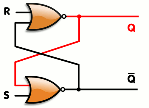
Another common type of circuit composed of the above described parts is the flip-flop, or latch. These circuits enable the storage of information. An example is the SR (set–reset) latch. Here is an interactive SR latch composed of individual switches: Interactive diagram by DrJolo (click link, then click on diagram to interact)
An SR latch can also be made from logic gates:
![]() Animated diagram by Napalm Llama, used under CC-BY 2.0
Animated diagram by Napalm Llama, used under CC-BY 2.0
Several flip-flops connected together and sharing a clock form a register, which is a form of memory.
Clocking
To transfer data around between different flip-flops, they need a trigger signal. This is provided by the clock. A clock in a processor is a signal that alternates between on and off at a specific frequency. (It has nothing to do with telling the time of day—that is the function of a real time clock, which is not usually part of the CPU at all.)
In modern computer CPUs, the main clock frequency can get up to 2 to 4 GHz—that's two to four billion oscillations between on and off per second. However, there is often a clock generator circuit that generates clock signals at different frequencies for different parts of the CPU. For example, the front-side bus (which the CPU uses to transfer data in and out) is often clocked more slowly than the core(s).
CPU architecture and subsystems
There is a huge variety of different CPU architectures, all optimized according to different constraints and requirements. For just about any method of operation you can think of, there's been a CPU designed that works that way.
However, the subsystems commonly found in a CPU are the following:
Control unit
The control unit, or CU, manages the flow of data between the other subsystems, and provides them with control signals. Typically, the CU is what takes an instruction (described below) from the computer program that the CPU is executing, and breaks that instruction down into steps to be taken by the other subsystems. These steps can include fetching data from memory, sending it to the ALU and telling the ALU what to do with it, sending data to or receiving data from external hardware, and storing the results back in memory.
Some control units break down the instructions using hardwired circuitry, while higher-end ones use microcode. Microcode is basically a reprogrammable lookup table of what steps to perform based on a given instruction. Using microcode makes design and development of a CPU easier, and it enables higher-level instructions to be implemented, which makes assembly programming easier. Microcode also makes it possible to use the same instruction set across several microarchitectures (designs of the CPU's hardware subsystems). As well, it allows patches to work around hardware bugs in a CPU design.
Arithmetic logic unit
The part of the CPU that actually does the calculations is called the arithmetic logic unit, or ALU. The ALU takes operands (data to operate on, typically two operands at once, each of which is a binary number) and an opcode (the operation it is told to perform by the CU). It uses logic circuitry to perform the requested operation on the operands, and when it has done so, the result appears at its output.
The operations performed by the ALU are arithmetic (addition and subtraction, multiplication and division, incrementing and decrementing, negation) and bitwise logic (bitwise AND/OR/etc. and left/right shifts). Multiplication and division are often omitted from simpler ALUs, and were not available at all until the late 1970s. This is because arbitrary multiplication and division are more difficult to do at the binary hardware level. However, multiplication and division by powers of two is easy: simply shift the bits to the left or to the right. (This is analogous to multiplying or dividing by a power of 10 in the base-10 system most humans are more familiar with.)
The ALU also has some status outputs (commonly including carry-out, zero, negative, overflow, and parity, which all indicate properties of the output number, and are described in more detail in the Wikipedia article). These are used by the ALU for future operations or to control conditional branching (e.g.
ifstatements in higher-level languages).Floating point unit
Some CPUs include a floating-point unit (FPU, commonly called a math coprocessor back when it was a separate chip), which is optimized for working with floating-point (non-integer) numbers. Without an FPU, floating-point operations can be performed by the ALU with the help of software such as CORDIC, but this is slower.
Processor registers
Almost all CPUs include processor registers, which are a small amount of memory where the CPU stores pieces of data it is actively working with. Most CPUs have a few data and address registers for storing operands and outputs that will be used again soon, as well as some more specialized registers such as the program counter, which points to the address (location in memory) of the instruction currently being executed. There are also internal registers (registers not accessible to the user's program) such as the instruction register, which holds the actual instruction being executed (as opposed to its address). Some also have control registers, where specific bits in specific registers control the operation of hardware features such as switchable clock speeds.
Instructions and assembly languages
Above, I mentioned instructions. Instructions are names for specific operations that a CPU can perform on data. A collection of instructions is called machine code. Together, the instructions a given CPU supports make up its instruction set architecture (ISA). Each instruction may specify where to access or store pieces of data (processor registers, addresses in main memory), what to do with the data (such as arithmetic operations), and other operations such as choosing the next instruction to execute based on certain conditions (branching).
In traditional architectures, an instruction is composed of an opcode, specifying what operation to perform, and one or more operands, which are usually addresses of the data on which to perform the operation. Some architectures also allow an 'immediate value', which is similar to a literal in higher-level programming.
Assembly languages
An assembly language is a slightly more human-friendly language than machine code. Generally there is a one-to-one (or almost one-to-one) correspondence between the assembly language of a given architecture and its instruction set. The assembly language, however, is easier to read because it uses alphabetic mnemonics (such as
movmove a value from one location to another,jmpjump to new instruction location,jnzjump if not zero—a branch operation) for commands and registers, instead of binary opcodes and addresses. The assembly language is converted to machine code by a program called an assembler. Some assemblers support higher-level features such as function declarations and calls, macros, and even object-oriented programming.Until higher-level languages became popular in the 1970s and 1980s, assembly programming was the main way programming was done. Today it is still used when resources are very tight, when speed of computation is paramount, and also for programming of home-built processors. As well, many of today's high-level languages are compiled into assembly code by their compilers, which is then converted to machine code to run on the CPU.
Next post
In the next post, coming in the next week, I plan to cover modern improvements to the CPU, such as pipelining, caches, and branch prediction. If there's anything you'd like me to cover specifically, let me know in the comments. Also let me know what you think of this post.
The Hardware Side of Computation
An exploration of CPUs, GPUs, and FPGAs, and how they each perform computation