-
1st building block: input attenuation
06/29/2024 at 11:36 • 0 commentsPassive probes input attenuation
Typical passive probes have a switch that lets you change between x1 or x10 attenuation. Dave from EEVblog has an amazing YouTube video explaining how these probes are built and how the attenuation is obtained:
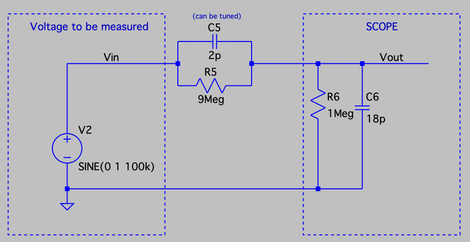
My oscilloscope has a 1 MΩ resistor with an 18 pF capacitor in parallel as input impedance, assuming that the passive probe has a 9 MΩ resistor in series (as shown in Dave's video), the equivalent circuit would be:
![]()
C5 is a variable capacitor (the flat screw seen on the probe) which is used to compensate this voltage divider, why?
Before answering this question, let's take a look at the circuit above. Basically is a resistive voltage divider with two capacitors in parallel. We know how a resistive voltage divider works, so why do we need these capacitors?
A resistive voltage divider works perfectly well at DC, but as we increase the frequency, the parasitic capacitance of these resistors will affect the response of the circuit, let's see an example:
![]()
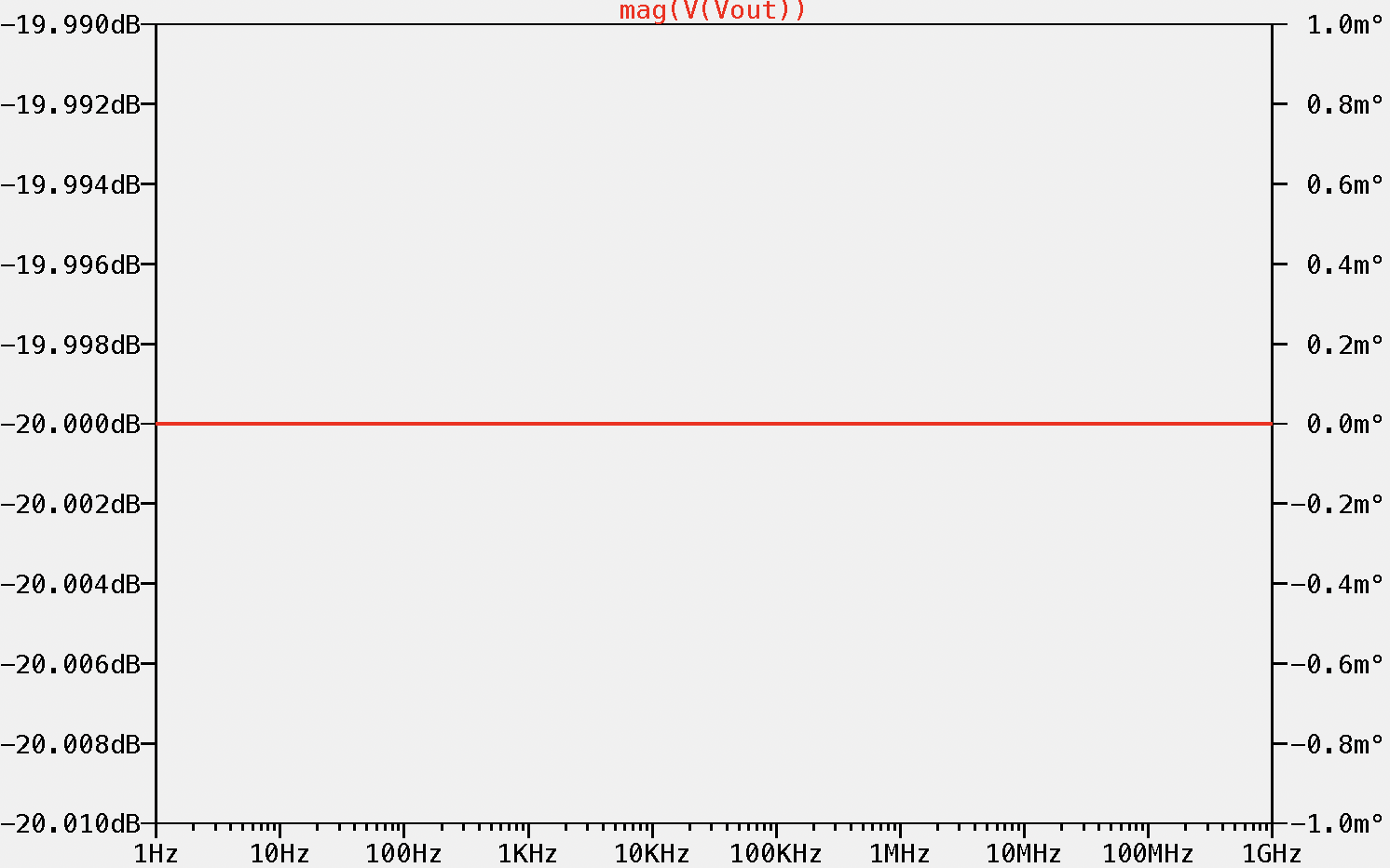
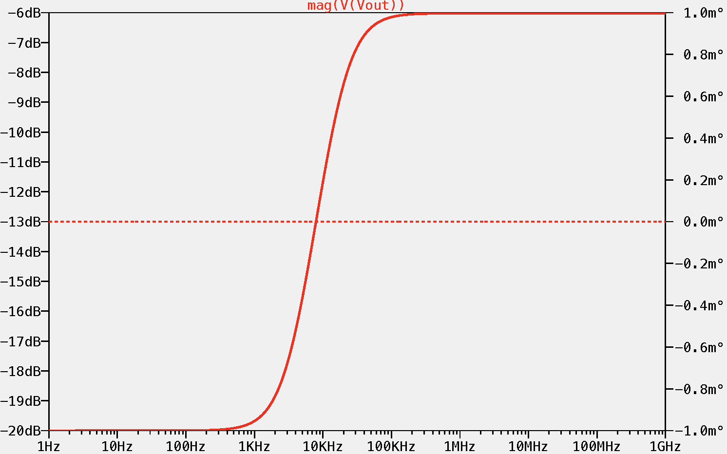
This is the frequency response of an ideal resistive voltage divider (with no parasitic capacitance). With R5 equal to 9 MΩ and R6 to 1 MΩ, the attenuation is 0.1 V/V (or -20 dB). Now let's see the difference when we add a 5 pF parasitic capacitance on both resistors:
![]()
As seen, the frequency response has changed drastically to a perfectly constant attenuation for all the frequency range to a change of the attenuation from -20 dB to -6 dB. This is not desired for an oscilloscope probe, as we do not want to modify the signal that we are measuring, so how can we solve this problem? With a frequency compensated voltage divider!
This Analog wiki article explains really well this type of voltage dividers (Analog Wiki link). Basically, a frequency compensated voltage divider is the circuit we have presented before, a resistive voltage divider with the capacitors in parallel, so how can we achieve this frequency compensation?
"The compensated divider employs pole-zero cancellation to suppress undesired frequency dependence caused by any stray capacitance on the output side of the network. If the resistor and capacitor values are adjusted so that the pole and the zero of H(s) are superimposed, |H(jω)| becomes independent of frequency." (from Analog Wiki)
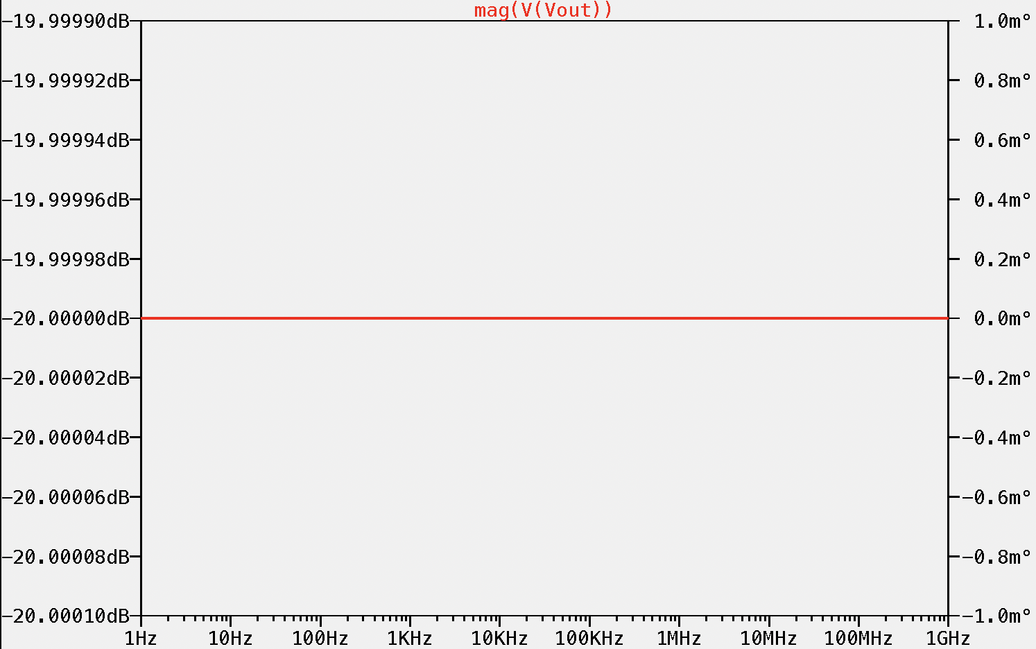
Basically, we have to fulfill that C6/C5 = R5/R6, easy! Let's try it, with R5 = 9 MΩ, R6 = 1 MΩ and C6 = 18 pF, C5 should be equal to 2 pF:
![]()
By using a frequency compensated voltage divider, we can obtain a constant attenuation regardless of the frequency of the input signal, nice!
"C5 is a variable capacitor (the flat screw seen on the probe) which is used to compensate this voltage divider, why?"
Basically, its function is to tune the value of the capacitor so the ratio C6/C5 = R5/R6 is fulfilled.
Differential probes input attenuation
Now, let's apply this concept to a differential probe. We know that we have to use a frequency compensated voltage divider to attenuate the differential input voltage of the probe, but why do we need to attenuate the signal? Can we just subtract both inputs and feed this voltage to the oscilloscope? Well, yes and no.
- Let's say that we want to measure the differential voltage of a shunt resistor used to measure current. The typical differential voltage swing across the shunt would be less than 1 V, which is inside the (typical) allowed voltage range of broadband difference amplifiers. Therefore, no attenuation is needed!
- Or let's say that we want to measure the Drain-Source voltage of a power MOSFET switching inside a power converter, with a typical differential voltage swing of 10 V. This voltage swing is much higher than the (typical) allowed voltage range of broadband difference amplifiers. Therefore, attenuation is needed!
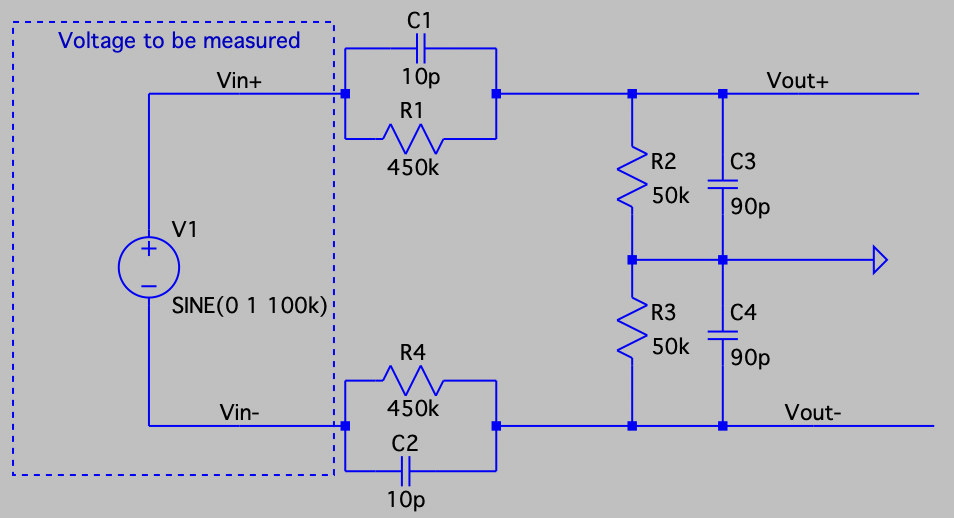
So, to be able to use this differential probe in both cases, we will add a -20 dB (x10) attenuation input stage. The basic circuit would be the following:
![]()
Aiming for an input impedance of 1 MΩ between inputs (as in Craig's project https://hackaday.io/project/191837-pd150/details) and an attenuation of -20 dB, we have set R1 to 450 kΩ and R2 to 50 kΩ, and considering that C3/C1 = R1/R2, C1 would be 10 pF and C3 90 pF. The frequency compensated voltage divider is the same for both inputs, and the input impedance between inputs is (450kΩ + 50 kΩ)·2 = 1 MΩ, as expected!
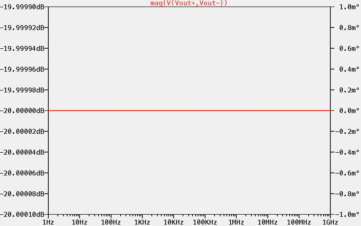
And this is the frequency response of the input stage:
![]()
But, not everything is as perfect as it seems. As passive probes have a variable capacitor to tune their frequency response, we also need to add tuning components to this input stage, because in a real implementation the resistors and capacitors would have a tolerance, and we also have to consider the input impedance of the broadband difference amplifier. Then, how can we modify this input stage so when we implement it in a PCB we maintain the constant attenuation regardless of the frequency? Basically, we have to add a potentiometer in series and variable capacitors in parallel to the frequency compensated voltage divider, so a fine tuning can be done when this circuit is implemented.
Okay, so basically with this special voltage divider and a couple of extra components for a fine tuning we would have a nice input stage, right? Well yes, but we can not forget about our precious friend in differential measurements, the common-mode voltage!
The common-mode voltage is a voltage that is present at both nodes of the differential voltage. Ideally, when subtracting the voltage of both inputs with a difference amplifier, the common-mode voltage will not be present at the output, but in reality, due to mismatch of the components used in the probe, an attenuated part of the common-mode would be present at the output.
Let's say we are measuring a differential signal which has 230 V of common-mode voltage, and that due to the circuit implementation we have a common-mode attenuation of -40 dB (0.01). Then, at the output of the circuit, we would have our differential signal plus 230·0.01 = 2.3 V!!!! Depending on the circuitry, this extra 2.3 V can cause distortion on the output of the amplifier.
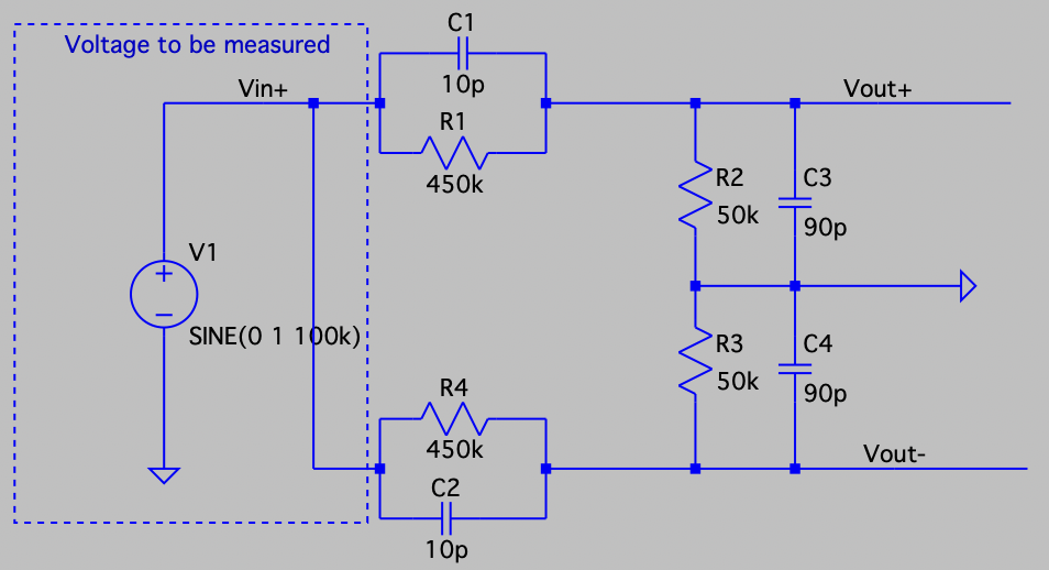
This "common-mode attenuation" is known as the "common-mode rejection ratio (CMRR)". In order to have a really large CMRR (to reduce to very low voltages the input common-mode voltage so it does not affect our measurement) the impedance between each input and ground has to be exactly the same, let's see an example:
![]()
We have modified the circuit to test the CMRR of our input stage. Let's see the frequency response:
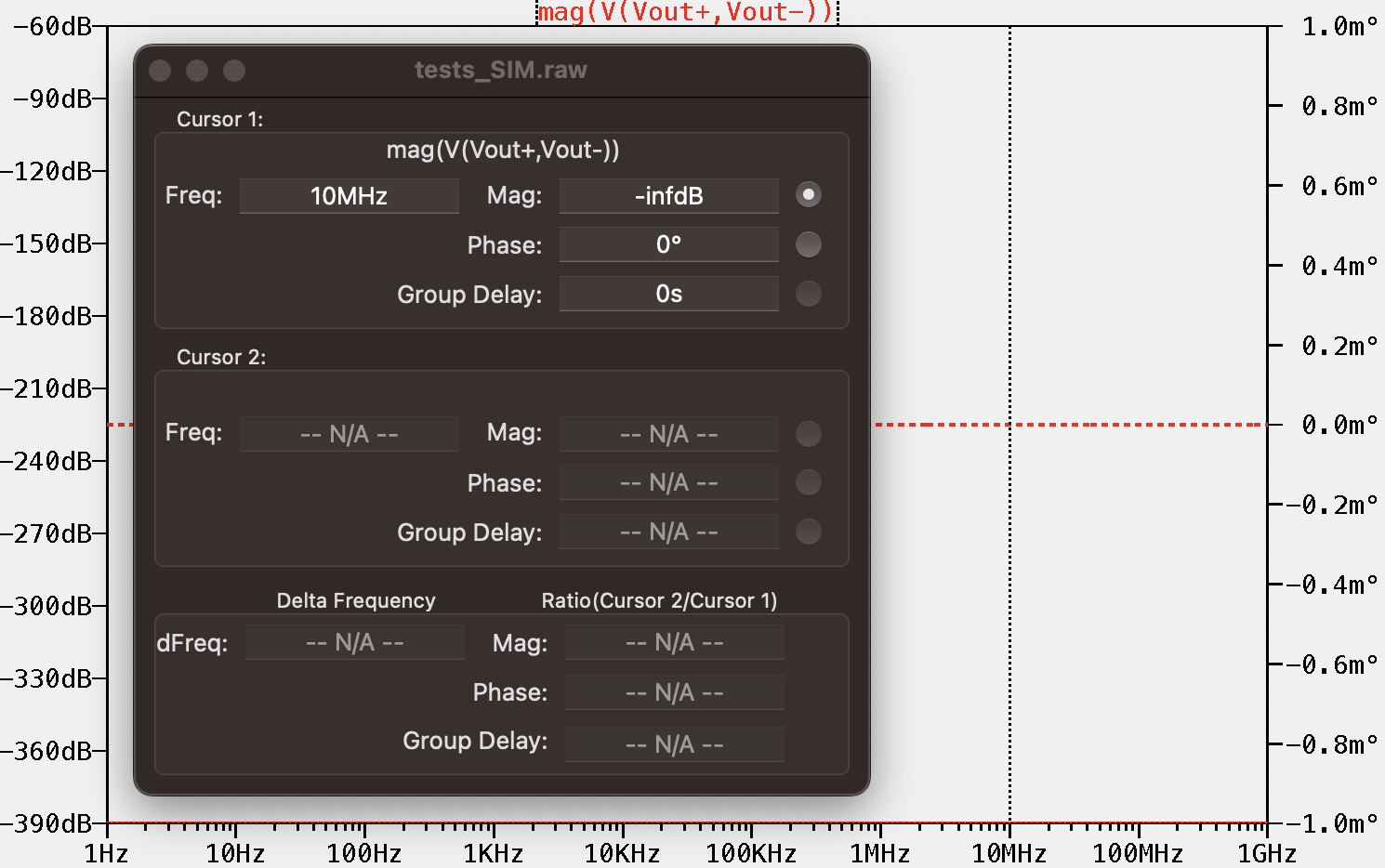
![]()
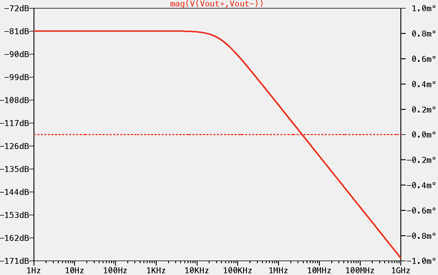
As we have perfectly symmetrical impedance between both inputs and ground, the CMRR is -∞ dB. Now let's change one resistor 0.1% of its value:
![]()
Just a 0.1% variation of one resistor has caused this reduction in the CMRR value. So, recalling what we have said before:
"Basically, we have to add a potentiometer in series and variable capacitors in parallel to the frequency compensated voltage divider, so a fine tuning can be done when this circuit is implemented."
The potentiometers would be used to adjust the CMRR and the low frequency response of the voltage divider, and the variable capacitors to adjust the high frequency response of the voltage divider. If everything is tuned perfectly, we would obtain a constant attenuation regardless the frequency and a good CMRR, nice!
 Miquel Tutusaus