PCB DESIGN
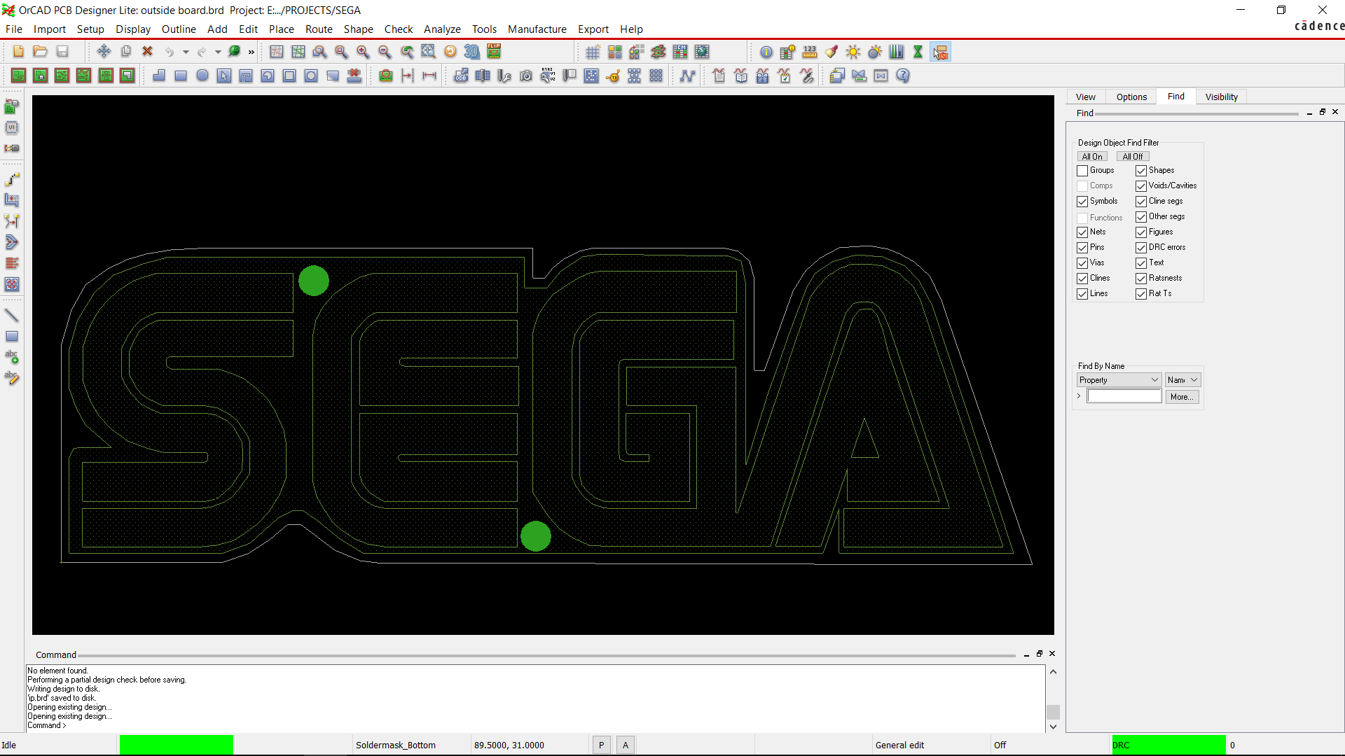
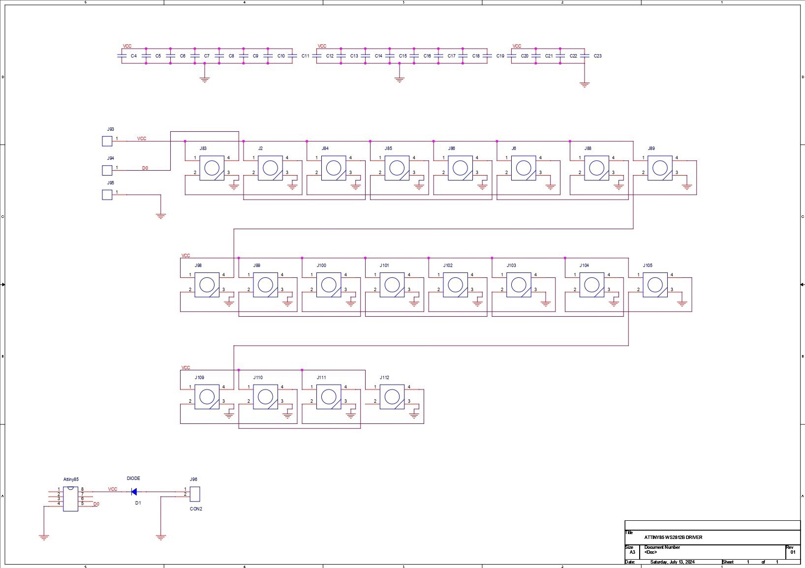
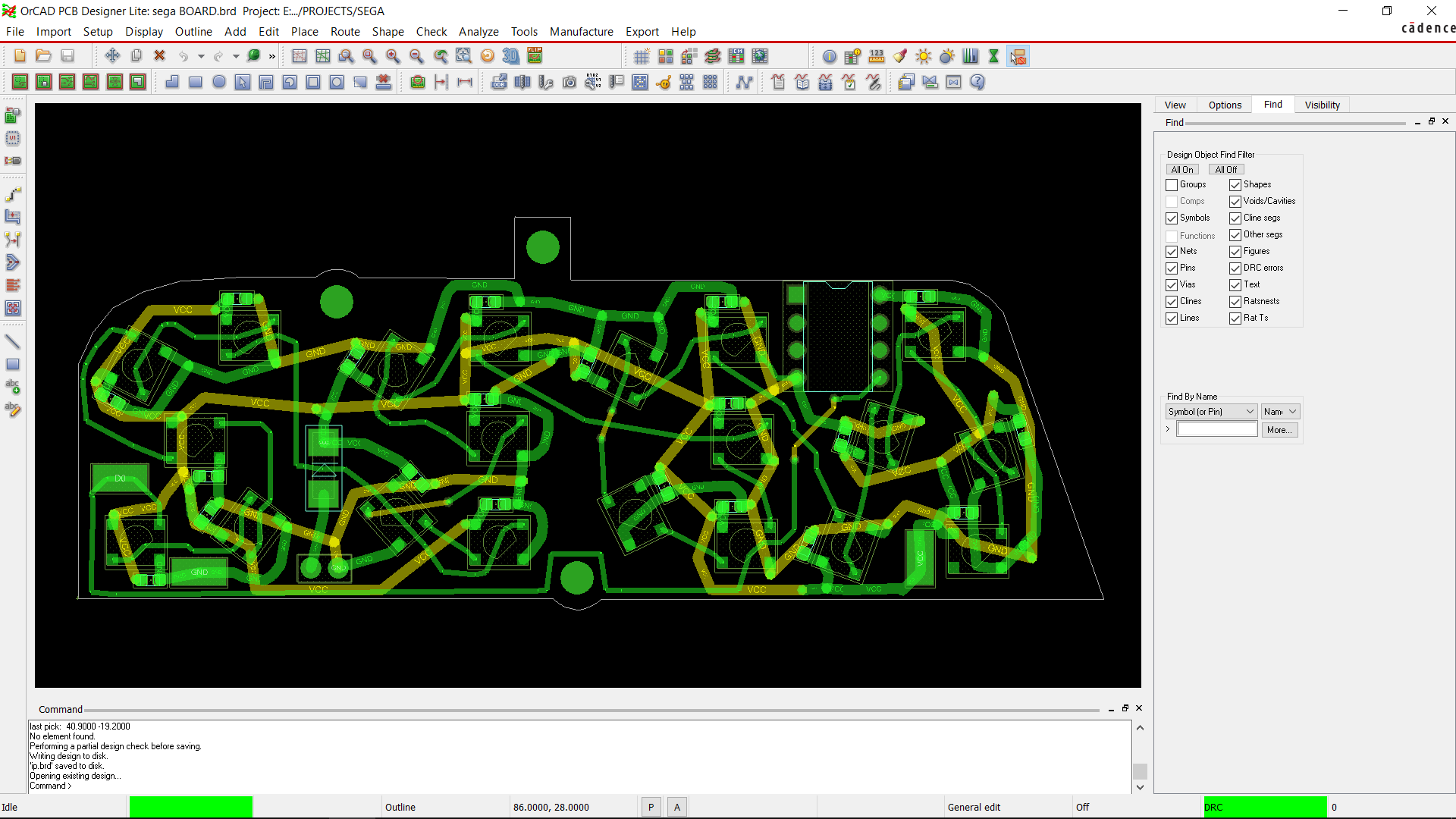
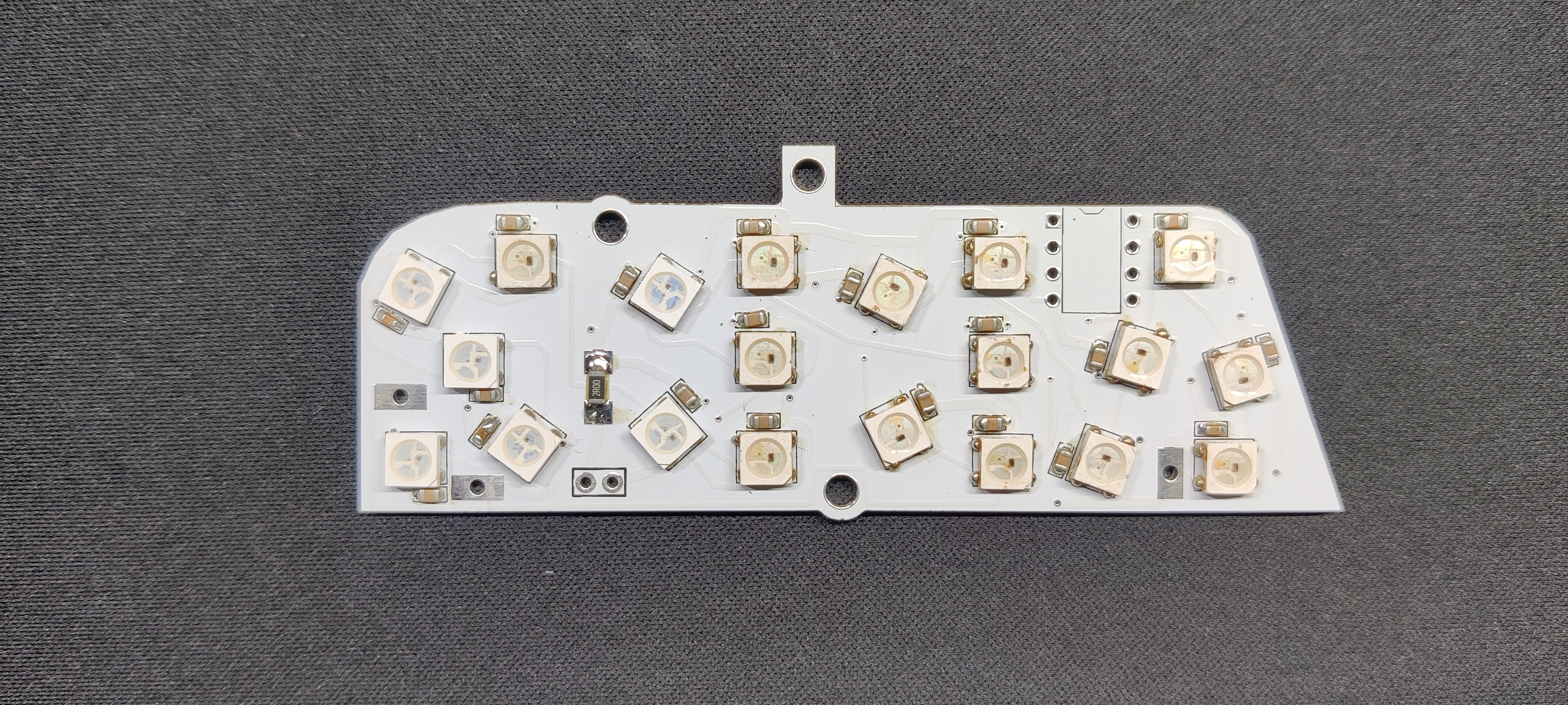
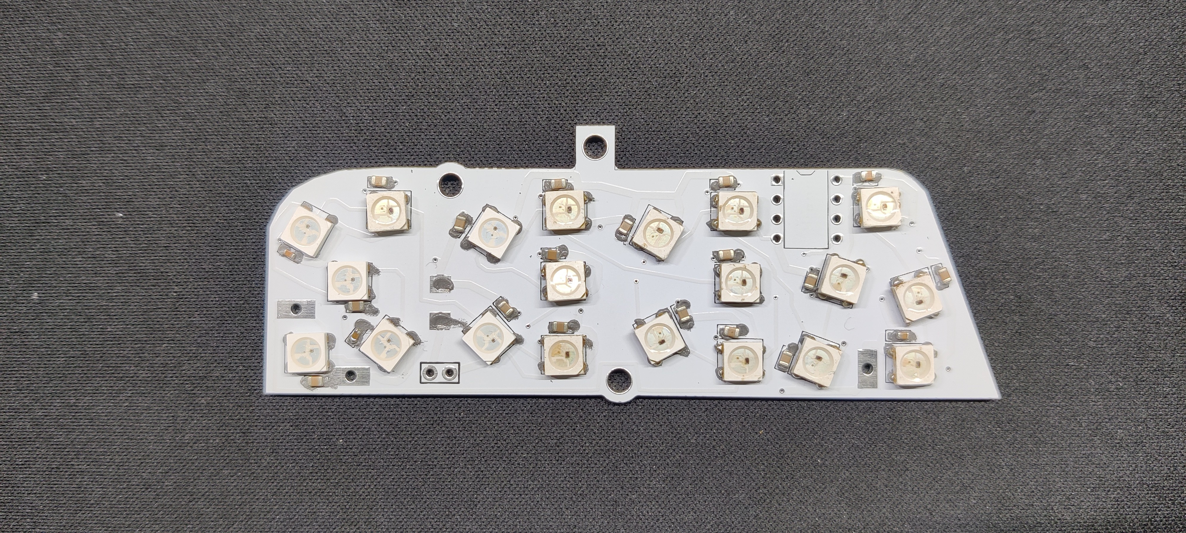
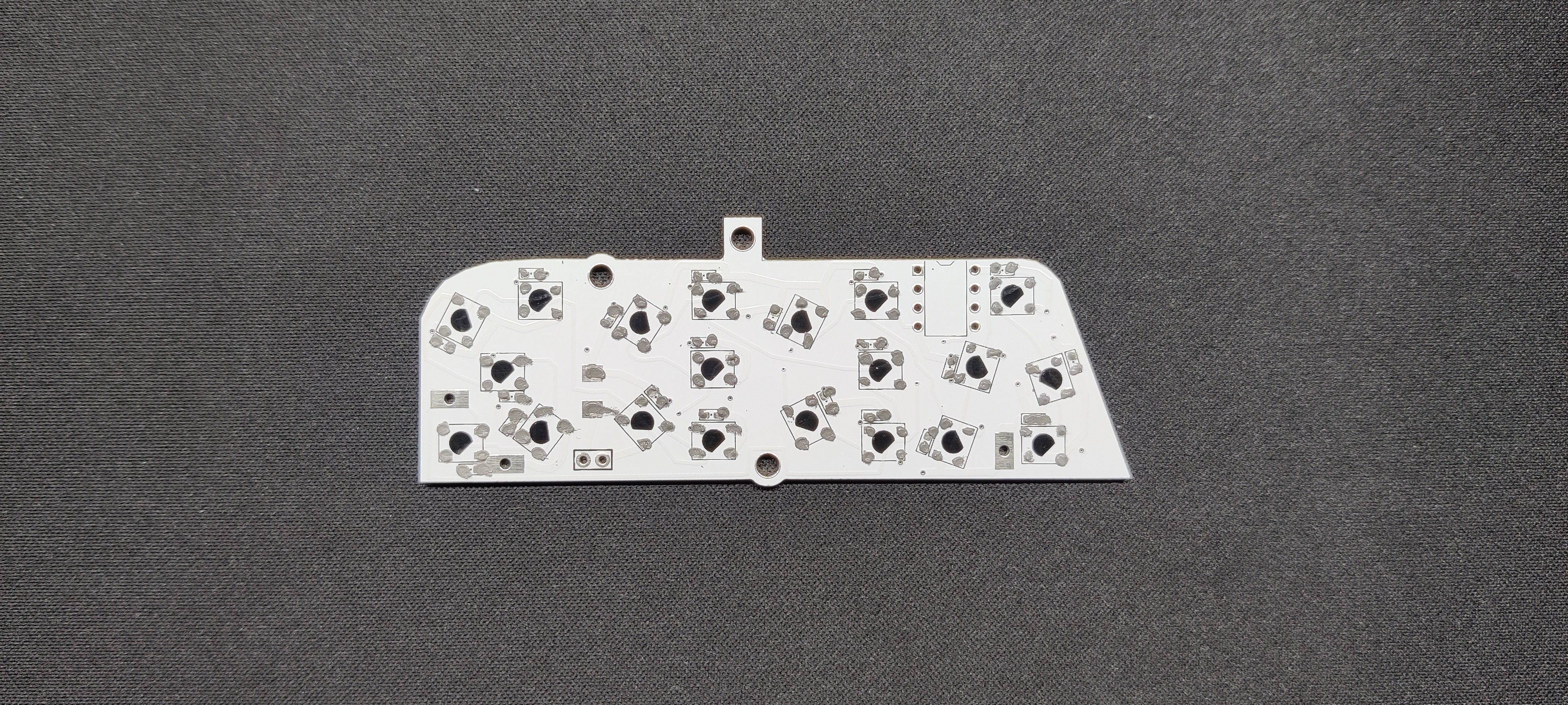
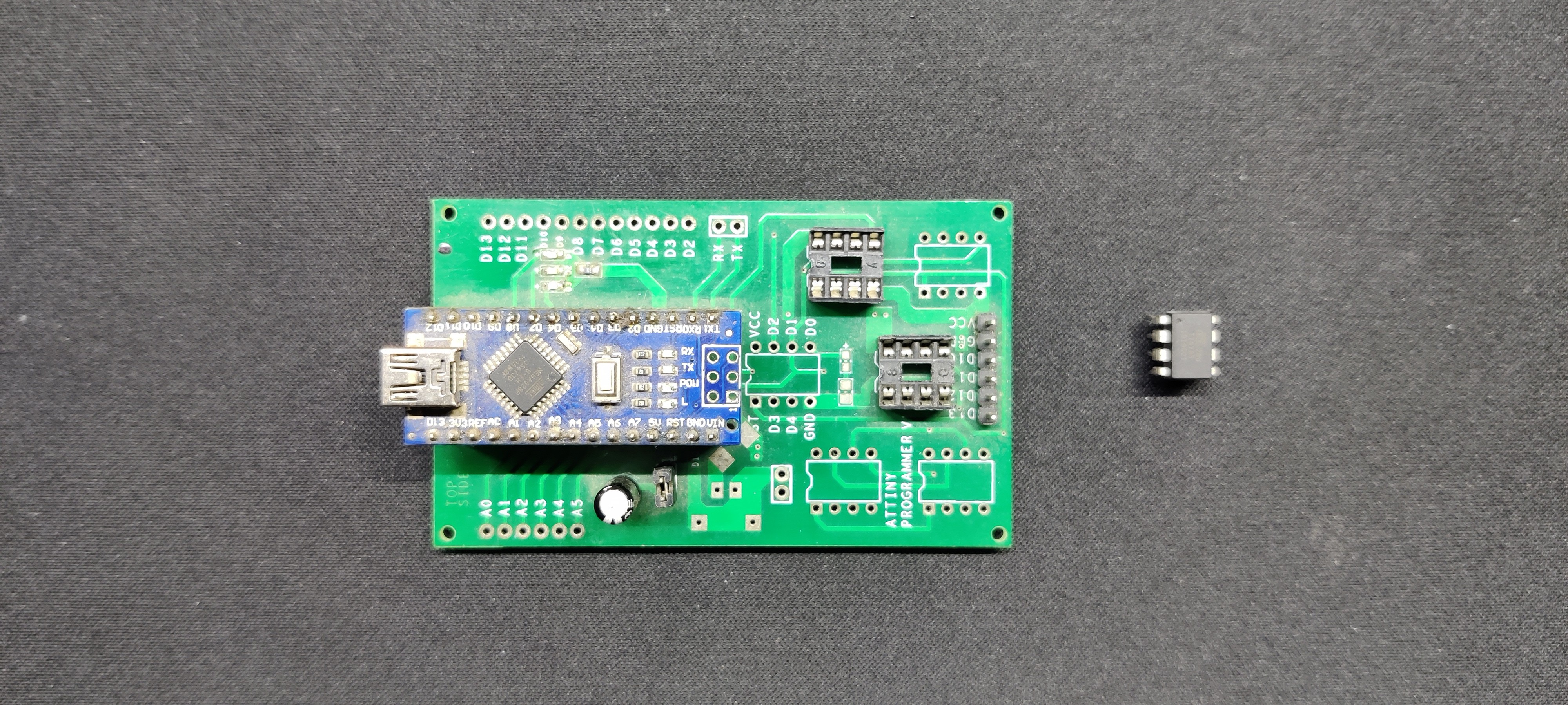
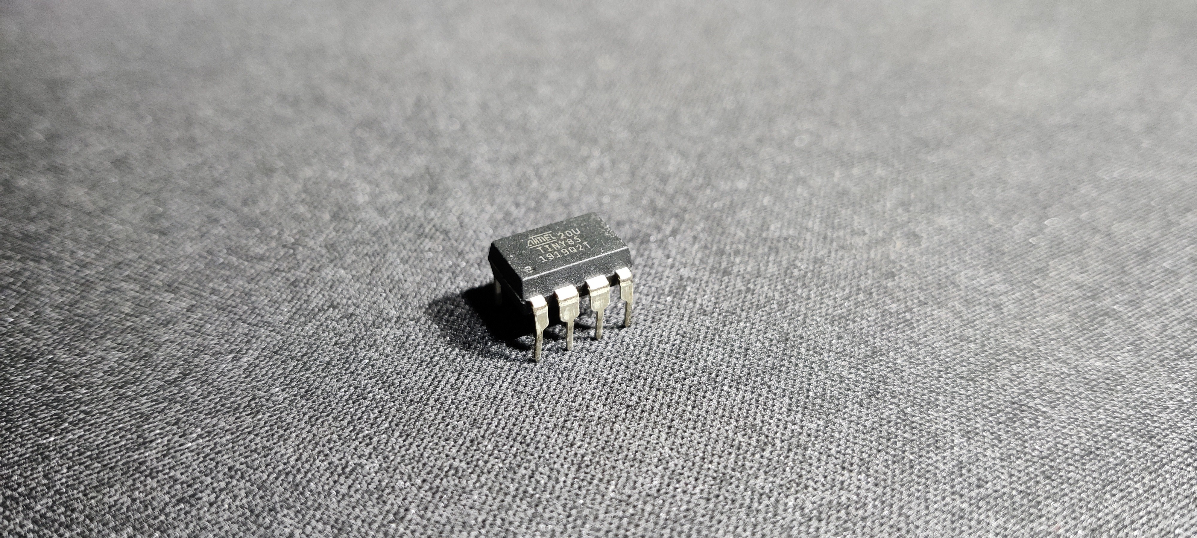
We started this project by setting up the schematic of the LED board, which consists of 20 WS2812B LEDs all connected in parallel with each other. The first LED's Dout is connected to the second LED's Din; the second LED's Dout is connected to the third LED's Din; and this goes up to the 20th LED. With Each LED, we have added a 100nf decoupling capacitor, which is stated as mandatory in WS2812B Datasheet and is to be placed as close to LED as possible. The 20 WS2812B LEDs are being driven in this instance by an Attiny85. Since our plan is to use an external programmer that will use a DIP8 socket to hold the Attiny85, we have not added a programming pin to this project. The programmer will then flash the Attiny85 with the main code. After that, we will take the Attiny85 out of the DIP8 socket and attach it to our main PCB. We added a CON2 connector for power input, to which the positive and negative ends of a USB cable will be soldered. Following the completion of the design, we created the PCB design, which was made up of two files: one for the SEGA logo and the other for the driver board. Since our Cad software only allows for the import of BMP images into the design, we first searched for a black and white image online and eventually found one. For the project to get started, we first created the circuit board and outlined the SEGA letters. Once the SEGA picture was taken off the board, LEDs were positioned inside the letters, resulting in a circuit with LEDs positioned right next to the Sega letters. Next, we removed every component from the design and re-added the SEGA picture using the same board file. Tracing the SEGA letters on the upper side of the solder mask opens it up. We took off the solder mask entirely on the bottom side. The solder mask can be removed to reveal light coming from underneath. Two boards were finalized and then sent to Seeed Studio Fusion for samples.
Seeed Studio Fusion Service
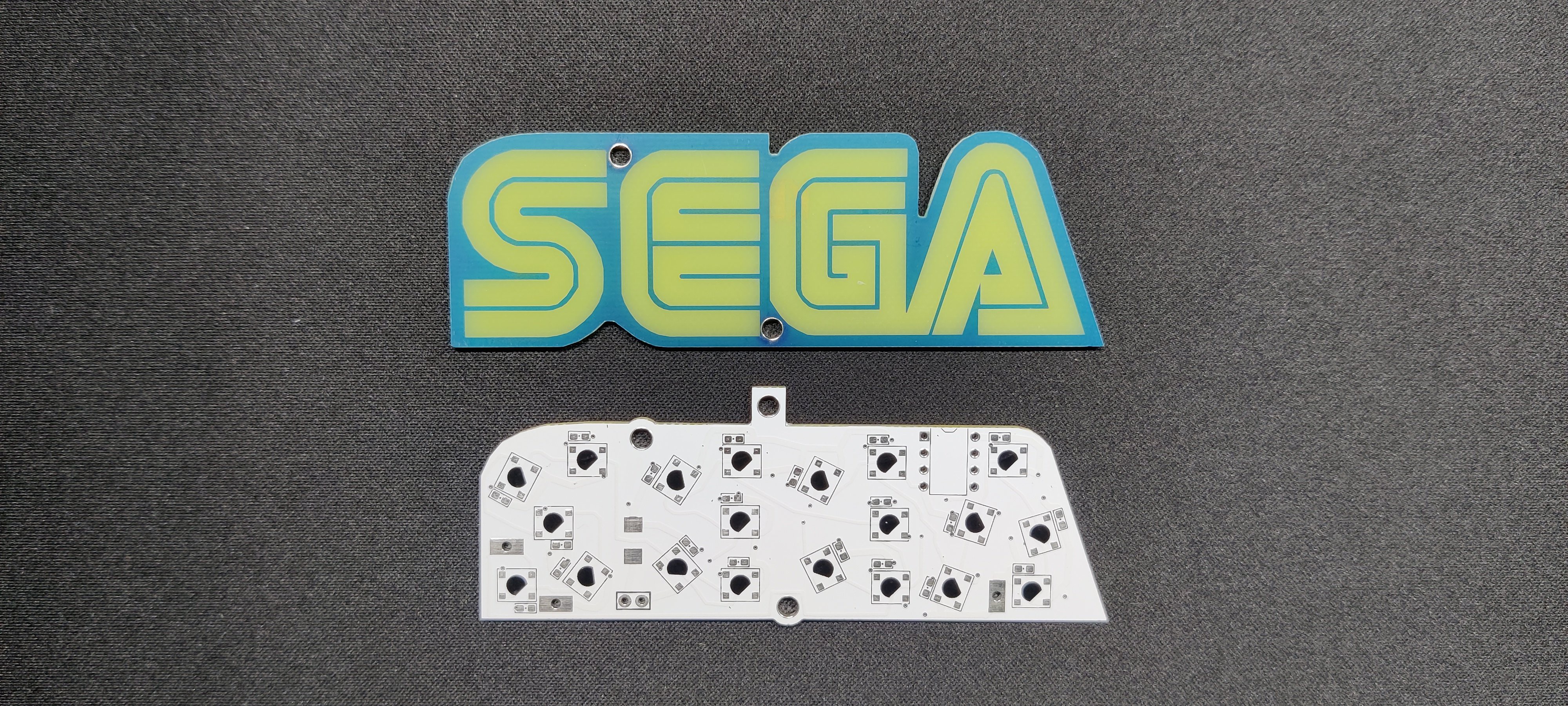
For this project, we are using two PCBs, which were provided by Seeed Studio.
Two PCB orders were placed, one for a blue-solder mask with white silkscreen and another for a white-solder mask with black silkscreen.
The quality was super good considering the rate, which was also pretty low.
Seeed Fusion offers one-stop prototyping for PCB manufacture and PCB assembly, and as a result, they produce superior-quality PCBs and fast-turnkey PCBA within 7 working days.
Seeed Studio Fusion PCB Assembly Service takes care of the entire fabrication process, from PCB manufacturing to parts sourcing, assembly, and testing services, so you can be sure that they are getting a quality product.
After gauging market interest and verifying a working prototype, Seeed Propagate Service can help you bring the product to market with professional guidance and a strong network of connections.
 Arnov Sharma

 sky-guided
 Oakmizer