Overview
Memory and I/O Emulation
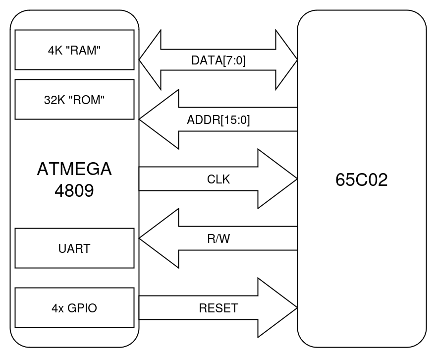
VR65C02 is a fully functional computer system. The ATmega microcontroller provides emulated RAM and ROM as well as a passthrough UART and four GPIO pins that the 65C02 can access.
The microcontroller controls the RESET and CLOCK lines of the CPU, so all memory access is handled synchronously by the Arduino code. For each bus cycle, the microcontroller reads the address bus and R/W pin from the CPU. If the CPU is reading a memory address, the microcontroller will decode the address into a memory value or an I/O operation and write the appropriate value out to the data bus. On a write cycle, the microcontroller reads the data bus value into its simulated RAM or updates the appropriate I/O system. The microcontroller implements address decoding in code in a similar way to a traditional system using logic gates or PLDs.
Both RAM and ROM are backed by large byte arrays in the microcontroller's memory, the RAM using onboard SRAM and the ROM using onboard Flash.
The UART is a memory-mapped I/O device from the perspective of the 65C02, similar to a 6551 ACIA. The CPU can read and write bytes and the microcontroller passes them through to one of its native serial ports.
Similarly, there are four GPIO pins accessible as a memory-mapped register to the 65C02.
Memory Map
The memory map of the 65C02 is as follows:
- 5KB "RAM" at 0x0000
- I/O regisers at 0x7F00
- 8KB "ROM" at 0xE000
The ATmega4809 has enough flash memory to support up to 32KB of ROM if necessary, but the total onboard SRAM is only 6KB and some is set aside for the Arduino code.
Software
The core of VR65C02 is the Arduino sketch running on the ATmega4809. As described above, this program simulates the entire bus cycle of the physical 65C02 CPU and all of the memory and I/O interactions.
Real 65C02 machine code is running on the CPU. This can be assembly or C code compiled with cc65. Since there is no physical ROM or RAM, the code has to live somewhere. My approach is to use the large amount of onboard Flash memory of the ATmega to store this. The main trick of VR65C02 is taking this compiled binary and getting it into the microcontroller Flash as part of the Arduino sketch upload.
The build process is done in a single script (build.sh). The process looks like this:
- Compile 6502 C code into a binary ROM file.
- Run a Python script to convert this binary file into a C header file with a large const array of bytes.
- Compile the Arduino sketch with this generated header file.
- Upload Arduino sketch to microcontroller with new 6502 code.
Programming the ATmega (and by extension the 65C02)
The ATmega4809 is programmed via UPDI, specifically, I am using a standard FTDI USB-serial adapter (with a 4.7k resister between Rx and Tx) and the SerialUPDI programmer in the MegaCoreX Arduino board package. Since the 6502 code is uploaded as part of the Arduino sketch, it's almost like programming a 6502 as an Arduino.
Limitations
All of the limitations of this system come down to hitting the limits of the ATmega4809 itself in one way or another.
Clock Speed
The main drawback is obviously clock speed. Simulating the whole bus cycle and all of the potential memory and I/O operations of the 6502 on a 20 MHz 8-bit microcontroller is not exactly quick. Measuring the PHI2 output on the CPU with an oscilloscope shows that the effective clock speed is about 257 kHz. Even at this speed, VR65C02 is surprisingly usable for simple GPIO tasks or interacting over the serial port, but it's about 4x slower than a Commodore 64 or Apple II.
Because not all the emulated peripherals respond at the same speed, the effective clock speed is actually somewhat variable depending on the I/O demands of the 6502 code. This doesn't fluctuate too dramatically, but heavy I/O, e.g. polling the serial port, will run at around 257 kHz, whereas no I/O at all will get the clock up to about 270 kHz.
Not Enough Pins
Besides the slow speed, the other main...
Read more » Colin M
 will.stevens
 Jim Jagielski