 Vitalii
1 Sources of inspiration
As you probably know, there are a myriad of different kinds of nixie clock on the internet. You can easily find schematic for clock with any types of nixie tubes. However, schematic of all this clocks is kinda similar and the main component in them is Arduino or other microcontroller. Obviously, the main advantage of such solution is simplicity – you can easily implement various functions in your clock, like settings, alarm, digits transitions and so on. Basically, the most simple and common nixie clock requires the next components:
- Arduino UNO
- RTC module DS1307
- nixie tube driver k155id1 (К155ИД1)
Despite being very simple and affordable, to me such circuits look too basic, probably, they could be more useful and helpful for beginners, who have just started studying electronics or for those, who don’t wanna bother with schematics and want simple and reliable solution.
In order to challenge myself, I decided not to use microcontrollers and RTCs, instead I assumed it would be better to use discrete microchips like it was back in the 60-s and 70-s. I remember how once in my university I was given a task to design a digital clock on binary counters on Verilog for FPGA. The code was pretty straightforward – binary counters were counting upwards till their maximum value after what they reset back to 0. Totally, there ware six counters each for one digit and they all were connected together in series, after previous counter resets the next one increments its value. For some reasons I found such a schematic very attractive, probably because of its simplicity. After a while I decided that it would be great to build this circuit using real components and not on 7-segment displays but something more attractive.
Another source of inspiration for this project were nixie tubes that I had. Every time I watched at them I thought how grate it would be to make digits in this tubes glow again. This clock has four IN-12 tubes, two for hours and minutes, and two IN-17 tubes for seconds. In the internet there are not a lot of variations of clocks with big digits for hours and minutes and smaller ones for seconds, so I assumed that such disproportion in digits’ size would look interesting.
2 Schematic
In this section I will describe separate blocks of the clocks’ schematic to make it easy to understand. In general, there are four blocks:
- Clock control – block which supplies entire clock and provides inputs to set and show time;
- Clock core – basically the heart of the clock. It contains binary counters which count time. Also this block generates high voltage for nixie tubes;
- Clock mux – contains multiplexers that convert counters’ binary values into decimal numbers;
- Clock display – basically just a display made of six nixie tubes;
3 Clock control
Schematic of control circuit is shown on figure 1. As it can be seen this circuit is very straightforward. The main sub-blocks are: battery protection, DC-DC step-up converter to 5V, three buttons to set hours, minutes and seconds and “wake-up” circuit.
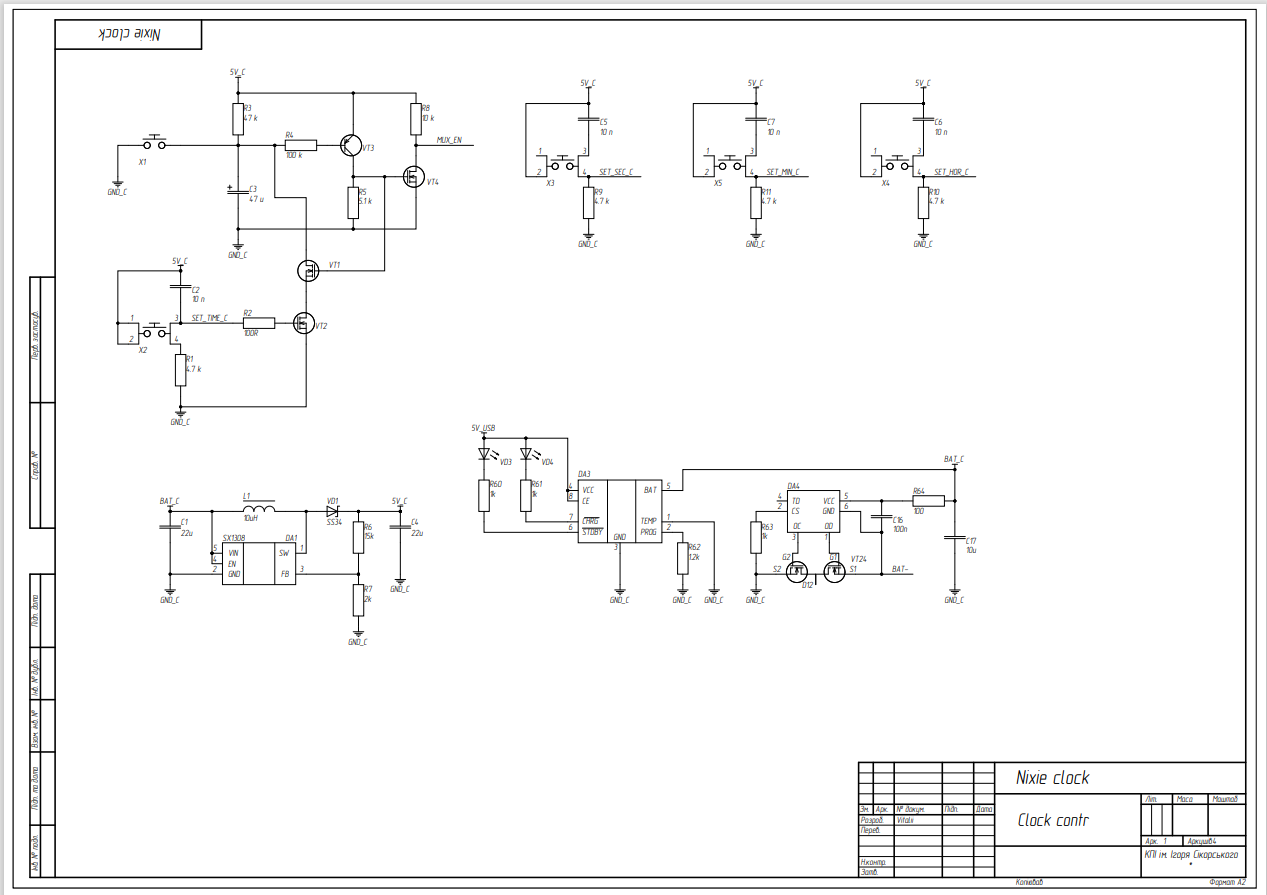
Figure 1.
Battery protection as mane suggests is needed to protect Li-Po battery from short circuits and over discharge. DC-DC converter provides 5V supply voltage for IC’s. The choice was made in favor of 5V because the high voltage binary to decimal converter K155ID1 (К155ИД1) needs 5V to operate properly, this component is crucial for displaying digits on nixie tubes.
Three buttons that “sets” hours, minutes and seconds control CLK multiplexers which sets CLK source for each of digit pair in clock. There are three digit pairs for every part of time (hours, minutes and second) and each consists of two digits – one digit represents most significant digit in number (aka tens of hours/minutes/seconds) and the second one represents the least significant digit (aka ones of hours/minutes/seconds).
The last sub circuit is “wake-up” circuit that is shown on figure 2.

Figure 2.
The purpose of “wake-up” circuit is to enable digits display on nixie tubes which includes generation of high voltage for tubes and enable of display driver. The signal which correspond to that is `MUX_EN`. This signal is generated by buffer that is formed from two inverters VT3 and VT4 which are connected is series. Signal `MUX_EN` is a repeated voltage on capacitor C3. When button X1 is pressed capacitor C3 immediately discharged and signal `MUX_EN` becomes low. After release of X1 capacitor slowly charges and level of `MUX_EN` remains low until voltage on C3 reaches buffer’s threshold voltage. Button X2 keeps capacitor C3 discharged when time is have to be set so indicators can show time as long as it is needed.
4 Clock core
Schematic of control circuit is shown on figure 3. Schematic for the core can be divided into three sub blocks: time counters, nixie tube display driver and high voltage generator.
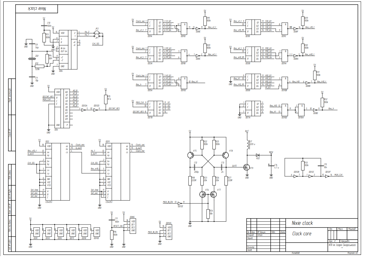
Figure 3
Time counter consists of binary counters H561IE10. Each IC has two 4-digit binary counter so one such IC can be used for one digit pair. On schematic it is shown that IC DD1 is used to count seconds, DD3 for minutes and DD5 for hours. To set reset value for each digit NAND gates are used. IC’s DD8 are tri state inverters and their purpose in this circuit is to generate power-on reset signal for all time counters. When power is just delivered to the circuit tri state inverters DD8 are in high-Z state and all counters are in reset state. Inverters remain in high-Z state until signal `RESET_SIG` reaches high level. After that inverters switch to normal mode operation and counters are no longer in reset state. All time counters are connected in series to each other which means that CLK signal for each counter is the reset signal of the previous counter except seconds counter DD1A for which CLK source is a 1Hz frequency generator DD6. In order to establish a setting function to the clock each digit pair can be clocked both from reset signal of previous pair or from 2Hz frequency generator DD6. CLK source selection for the counters is possible with help of multiplexers CD4053 which consists of three dual channel analog multiplexers. Each output of first multiplexers layer are connected to corresponding digit pair CLK source pin.Simultaneously one input of each multiplexer is connected to reset output of previous digit pair and another one is to output of the second “layer” of multiplexers. All multiplexers of first layer are drive by one signal SET_TIME which comes from “clock control” module. Simplified diagram of multiplexers connections is shown on figure 4.

Figure 4
Second layer is used to connect input CLK source of each digit pair to 2Hz frequency clock. Each multiplexer of second layer is driven by individual signals from “clock control” module like `SET_SEC`, `SET_MIN` and `SET_HOR`. In such way each digit pair can be set individually.
Display driver consists of counters DD4, DD7B and frequency generator DD12B/C. Counter DD4 is a decimal counter which implements dynamic indication and whoes module is set to 6 since display has only six digits. So each output of DD4 corresponds to each digit of the display – when level on one of the outputs is high a high voltage is applied to the corresponding nixie tube. Counter DD7B is needed to determine number of what time counter should be displayed. More specifically counter DD7A switches 4-bit channels of 6 input multiplexer in block “clock mux”, output of this multiplexer is connected to high voltage binary to decimal decoder K155ID1. Frequency generator powers conters DD4 and DD7B. Entire display driver is enabled only when `MUX_IN_EN` signal is set to low level which means that clock should show time.
High voltage generator is basically a simple step-up converter. PWM signal for the converters is generated by multivibrator on transistors VT5 and VT8. This generator also active only when `MUX_IN_EN` signal is set to low otherwise voltage on capacitor C14 repeats voltage of battery.
3 Clock mux
Schematic of clock mux block is shown on figure 5.

Figure 5
It contains four CD4051 8 channel multiplexer, high voltage decoder and six nixie tube drivers.
Multiplexers are needed to select which number from time counters should be displayed on specific nixie tube. Each multiplexes corresponds to specific bit in 4-bit number which will be send to the high voltage decoder. Each input channel of multiplexer is connected to the bits of time counters which has the same order of digit in 4-bit displayed number. For example, input channel of multiplexer DD14 from 0 to 5 are connected to the least signafacant bits of each time counters numbers since output of DD14 is connected to the least signaficant bit BIT0 of decoder. Selection signal `X1`, `X2` and `X3` of all four multiplxers are connceted toghether. Signals `X1-X3` for cjannel selection are generated by binary counter DD7B in block clock core. Signals `A0_BM` – `A5_BM` control high voltage keys which supplys anodes of nixie tubes with high voltage. Those signals are generated by counter DD4 in block clock core.
Finally high voltage decoder DD13 is supplyed via opto relay DA2 with 5V. Such a decicion was introduced in order to minimize power consumpliton of circuit when clock does not show time. Since IC K155ID1 is implemented in TTL logic it consumes a lot of current in stand by mode (approximately tens of mA). By using relay entire clock consumes around 100uA when time showing is disabled.
4 Clock display
Schematic of clock display block is shown on figure 6.

Figure 6
Display module consists from four IN-12 nixie tubes for displaying hours and minutes, two IN-17 nixie tubes for displaying seconds and two neon tubes to mark separating dots between hours and minutes. Dots are always suplyed vis resistor R59 when time is shown on display.
PCBs
PCBs for my nixie clock I designed in Altium Designer 20 and ordered manufacturing of them on JLCPCB. I must say that I was gladly impressed by the high quality of PCBs, black mask definitely gives clock a looks of polished product. Also it was a pleasant bonus that JLCPCB send not one but five sets of PCBs for the clock, so theoretically I can make four more nixie clocks, maybe for sale or maybe as a gift. In a future I will for sure order all my PCBs at JLCPCB.
