
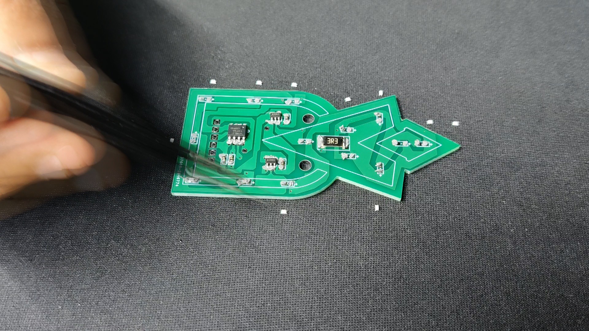
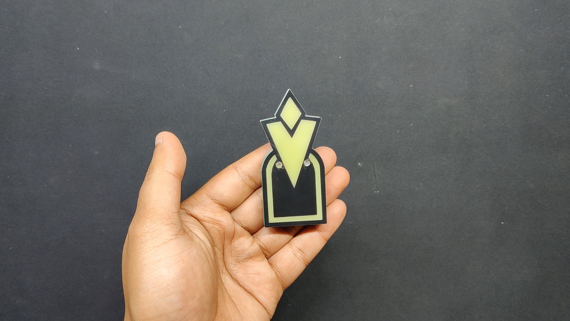
LEDs have been added to the bottom layer, and their glow is visible through the top layer because the solder mask top and bottom of the top layer have been opened from the area directly in front of the LEDs, allowing light to pass through the FR4 material of the PCB.
We are using the reliable Attiny13A 8-bit microcontroller as the brains of this project. It is connected via two Mosfets, each of which has a parallel array of LEDs.
PCB Design: Schematic
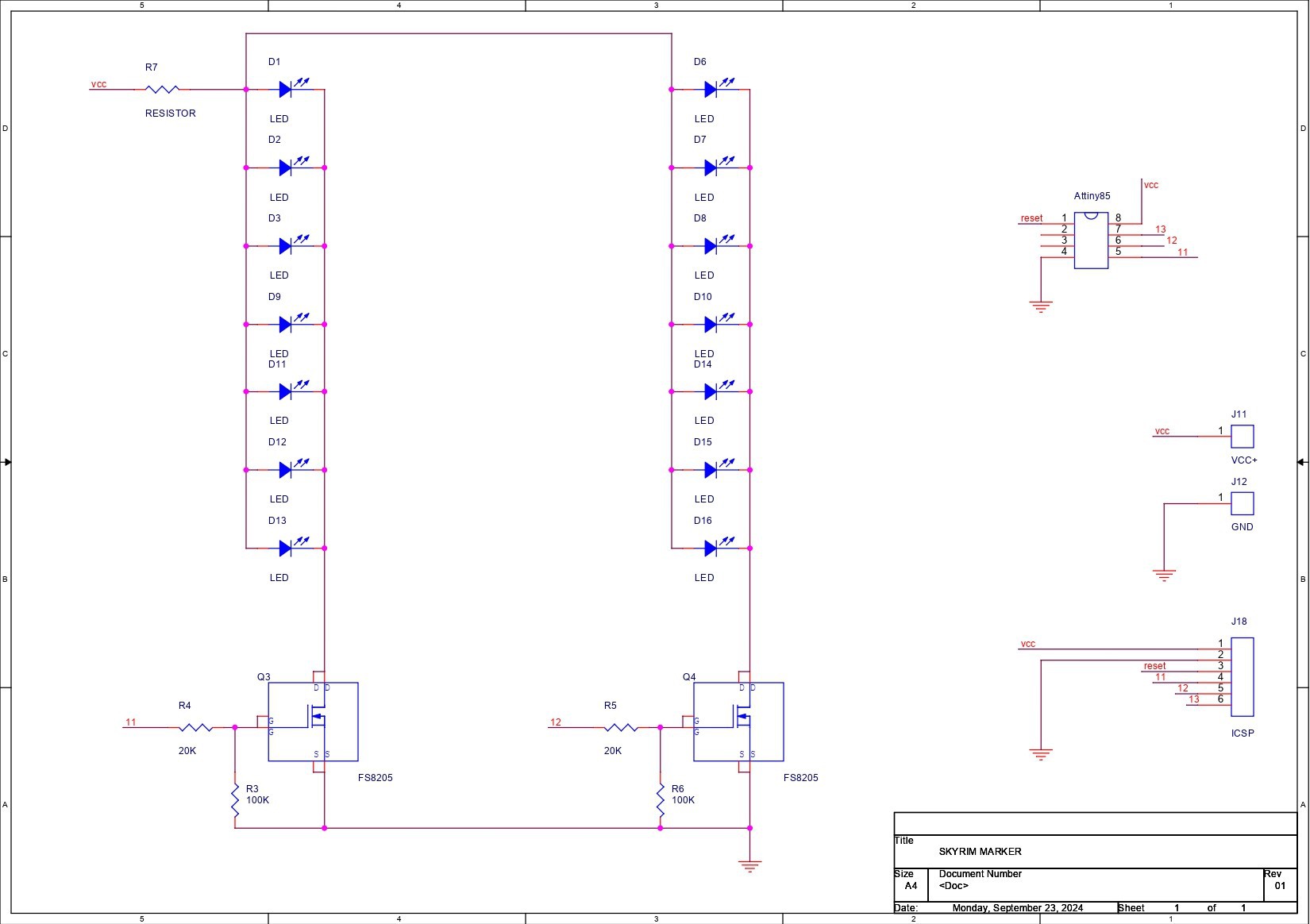

The first step in this project is to put together a schematic for the base layer,, which is an Attiny13A connected to two 8205S Mosfet IC Setups via 20K resistors, each of which is connected to the D0 and D1 I/O Pins of the Attiny13A.
Here, the mosfets are configured in "Mosfet as Switch" Setup.
In order to keep the gate pulled down when the MCU is not receiving any signals, we have also put two 100k resistors between the mosfet's gate and GND.
Seven LEDs have been added in parallel to each mosfet IC setup. The anode of each LED is connected to the setup's VCC via a 3R3 load resistor. All LED cathodes are connected to the transistor's drain.
We also added a CON6 terminal, which will be used as an ISP programmer for flashing the ATtiny13A with our previously built Arduino as ISP programmer.
We have added the ATtiny SPI pins, MISO, MOSI, and SCK, to the CON6 terminal along with the reset, VCC, and GND pins.
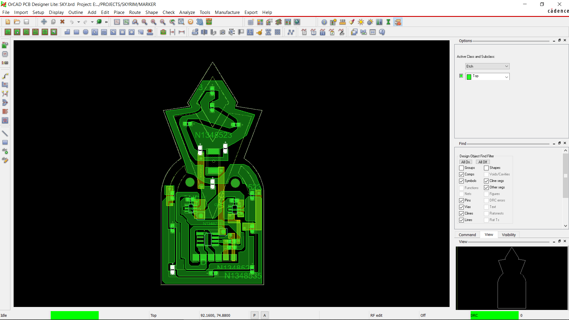
Once the schematic was finished, we imported a picture of the Skyrim Quest marker into the PCB design and used that to position all of the LEDs in the marker's white region in order to prepare the board design. This white space will be used to allow light to flow through by being opened up in other boards.
The microcontroller, resistors, mosfet, and CON6 Pad are placed in the center of the board, close to the marker's black region. Every component will have a slot created for it on the middle layer.
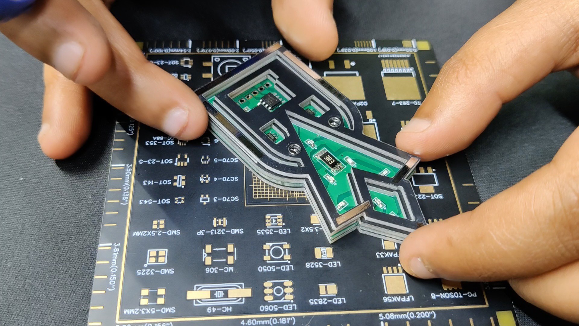
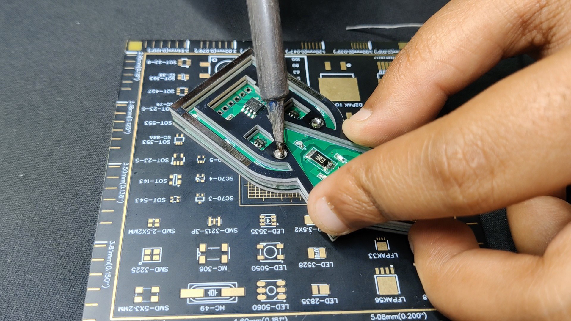
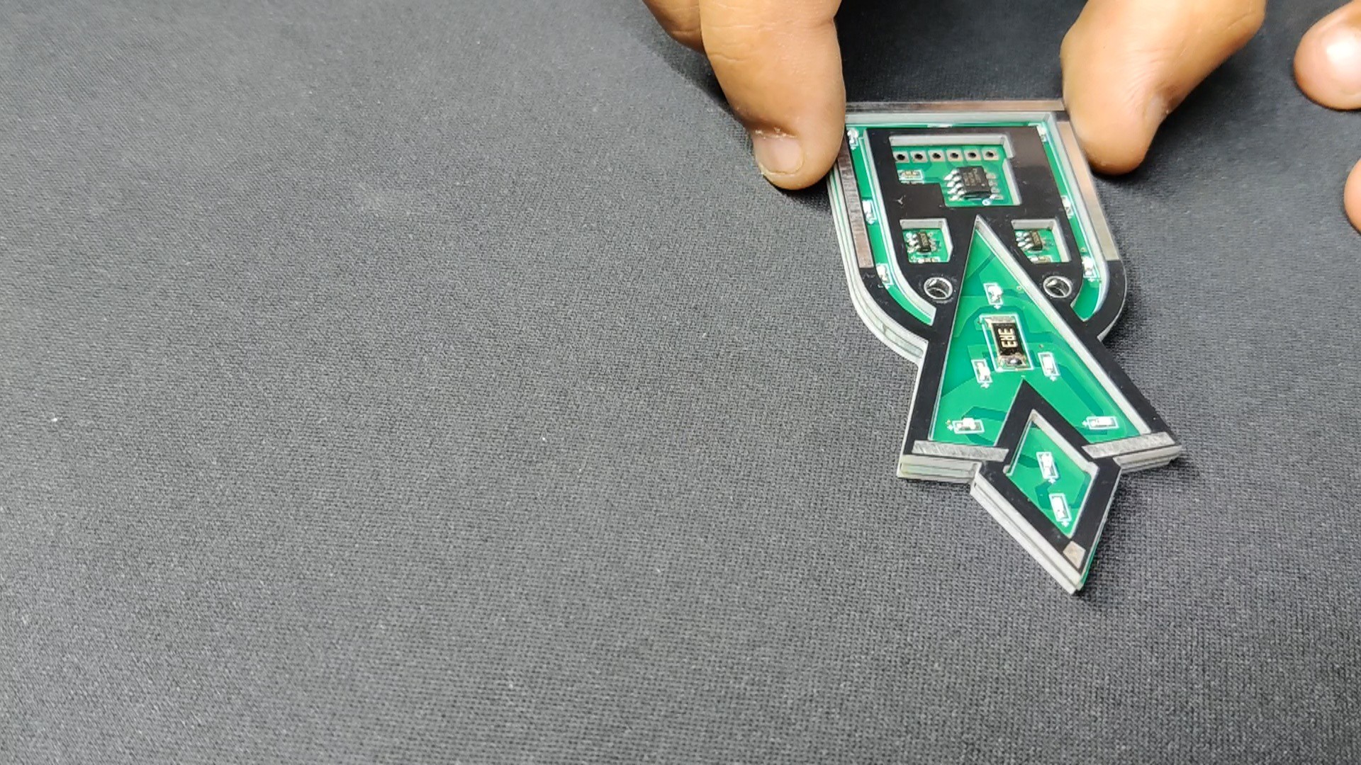
Two 4mm mounting holes were added in order to connect all the layers together. We can line up all of the layers consistently by stacking them on top of one another and aligning the two holes. Since the interior of these holes, will be plated, we can then use solder wire to join the layers together.
We connected all component tracks together in the right order and finalized the board.
PCB Design: Mid layer and Top layer
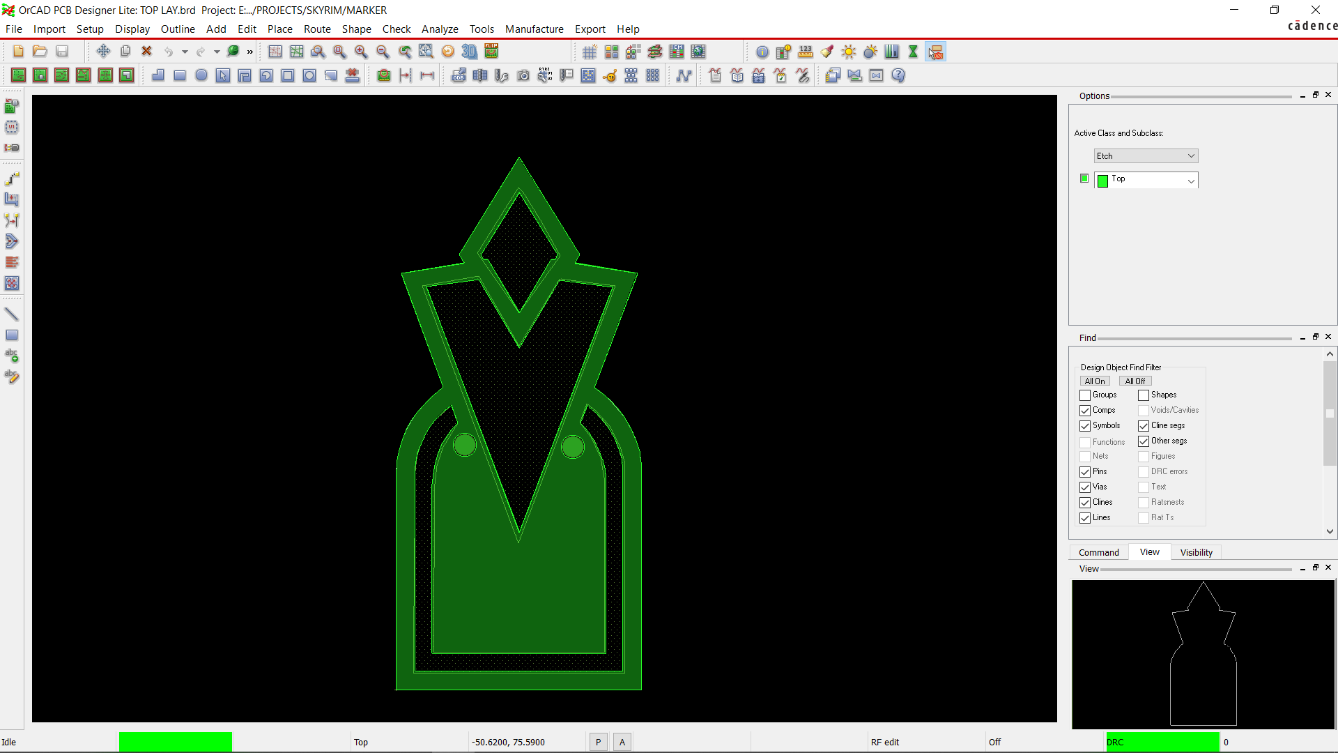
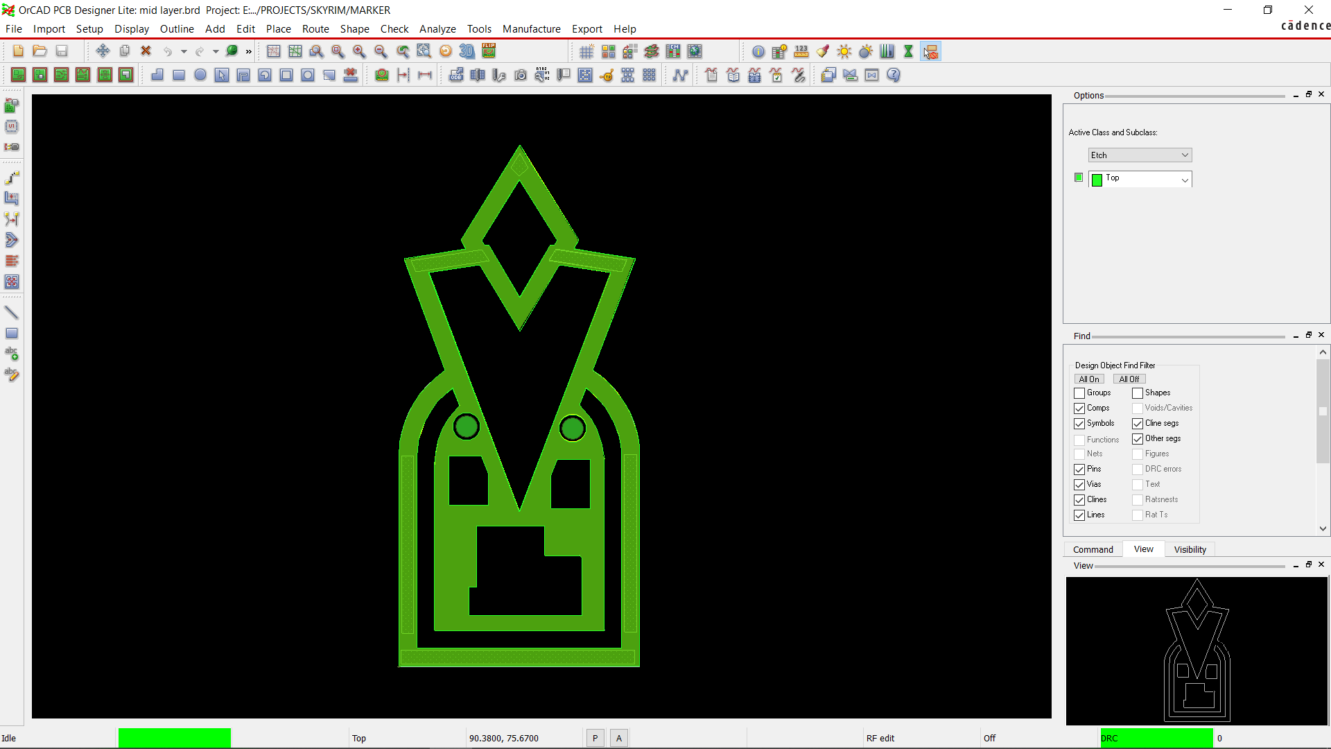
We created the top and mid layers, which are devoid of any components or traces, once the bottom layer was finalized.
Reusing the Skyrim Quest marker image from the bottom layer board, we first prepare the Mid Layer board, which had multiple slots and openings.
The board slot layer was used to completely open the white area in the image, which is where the LEDs will be placed.
A few slots have been added to the middle, where the microcontroller, resistors, and Mosfet IC are located, so that the Mid Layer board can be positioned on top of the bottom layer without coming into contact with the components.
On the top board, we added solder mask openings in both the top and bottom layers, which will allow the light to pass through the FR4 material.
HQ NextPCB Service
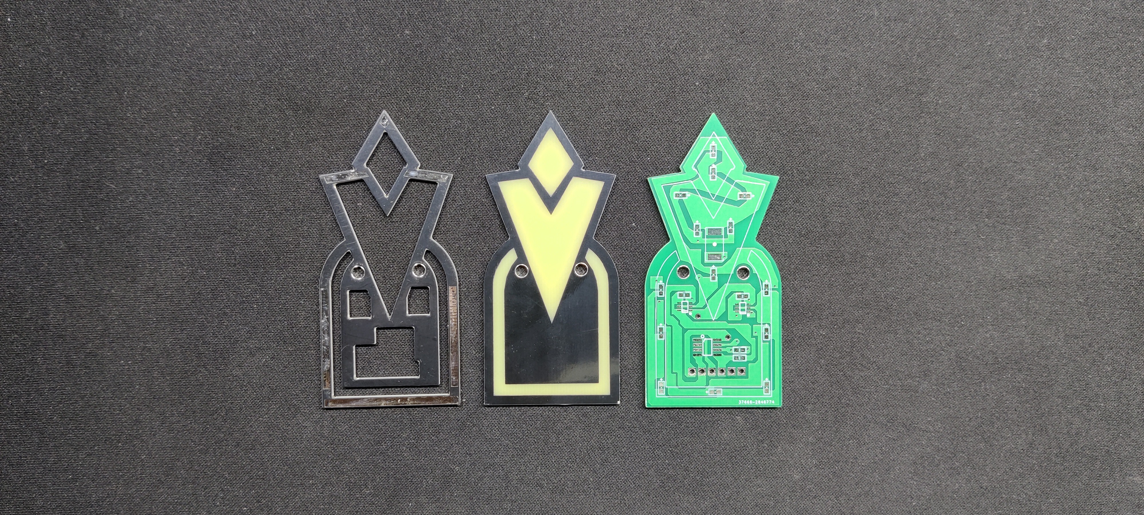
After completing the PCB design, we export the Gerber data and send it to HQ NextPCB for samples.
For the bottom, mid, and top layer boards, three orders were placed. We selected to use a green solder mask with white silkscreen for the bottom layer. We ordered Black Soldermask with White Screen for the Mid and Top Layer Board.
After placing the order, the PCBs were received within a week, and the PCB quality was pretty great.
In addition, I have to bring in HQDFM to you, which helped me a lot through many projects. Huaqiu’s in-house engineers developed the free Design for Manufacturing software, HQDFM, revolutionizing how PCB designers visualize and verify their designs.
HQDFM: Free Online Gerber Viewer and DFM Analysis Tool
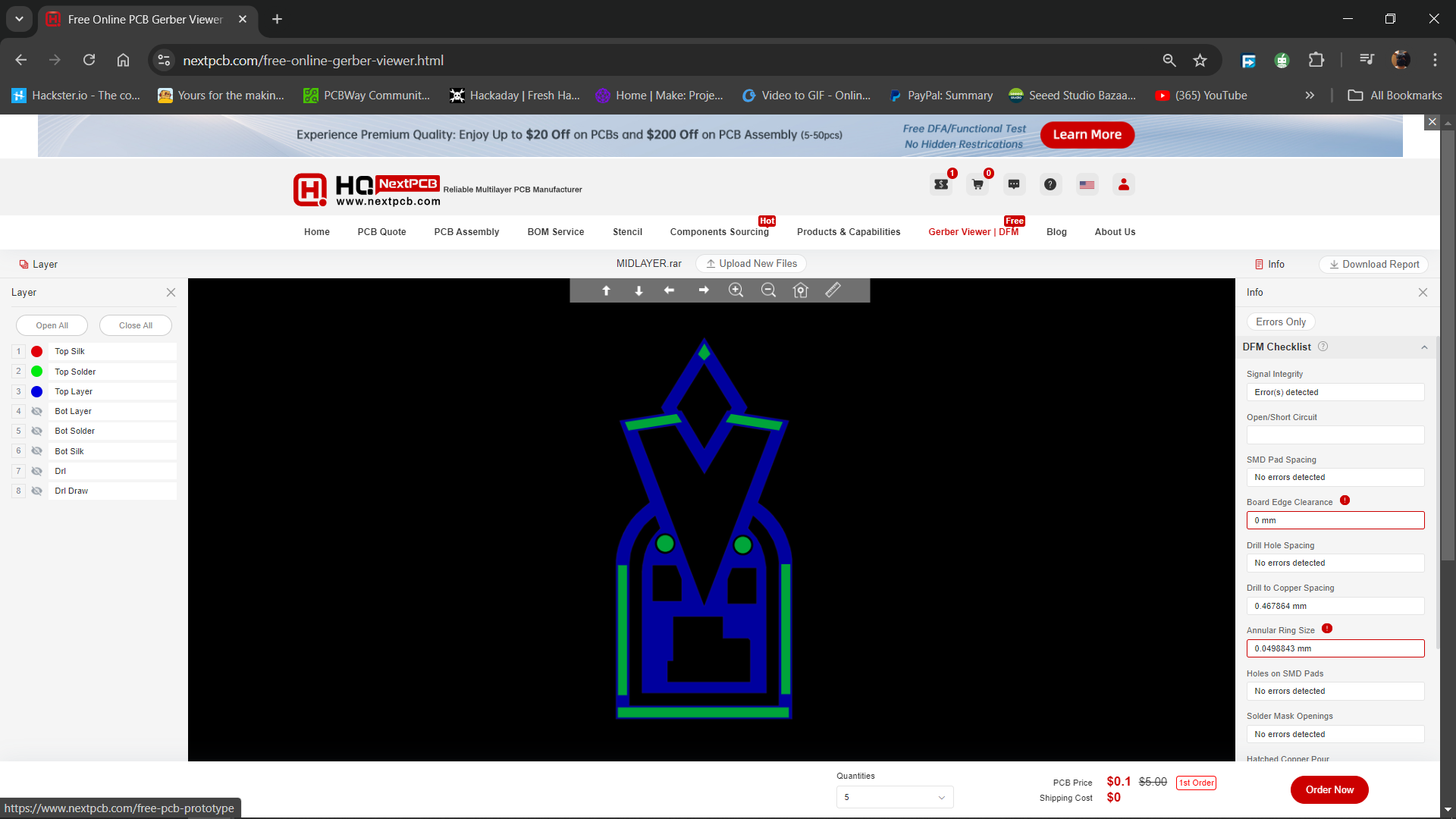
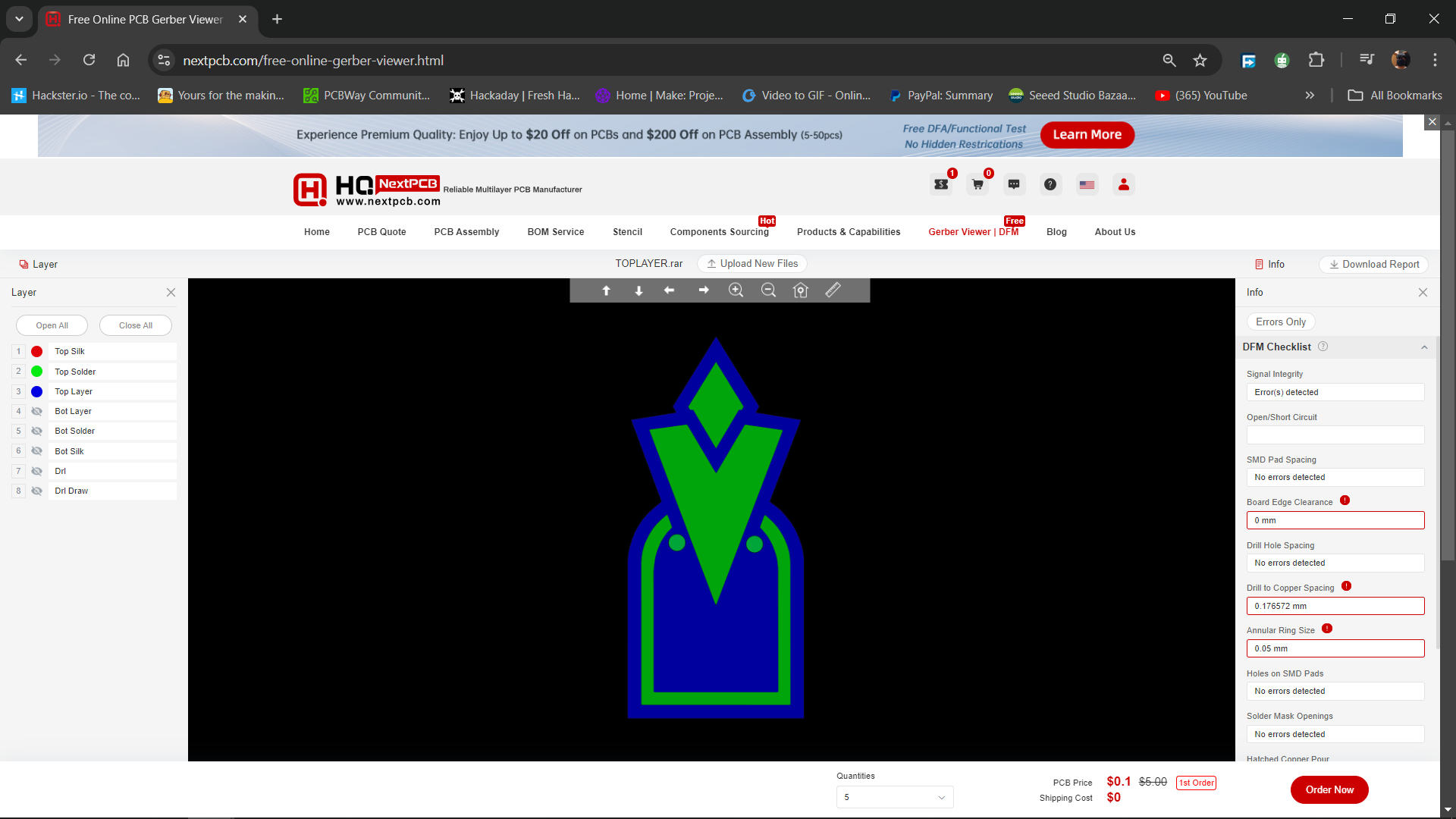
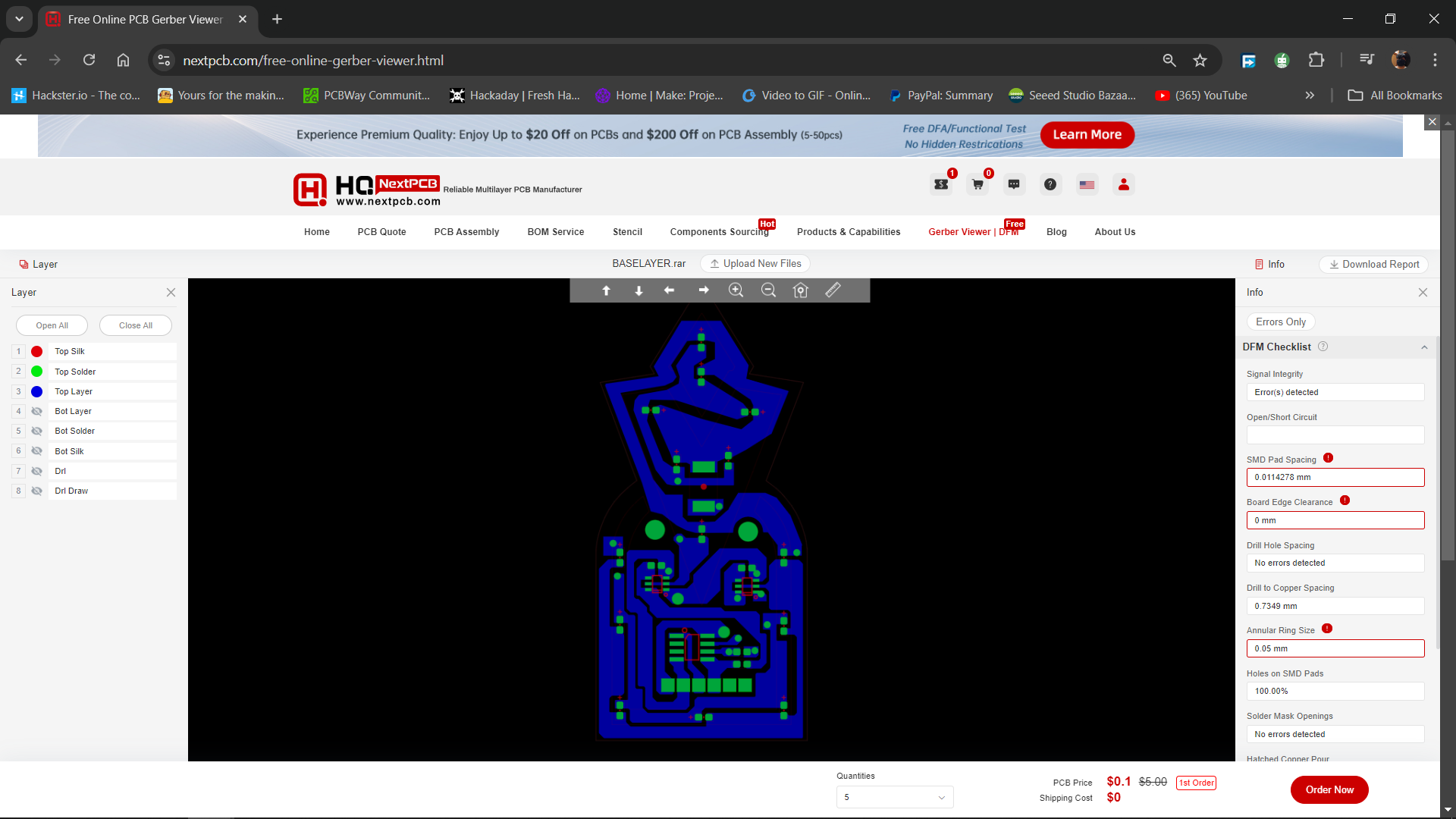
Also, NextPCB has its own Gerber Viewer and DFM analysis software.
Your designs are improved by their HQDFM...
Read more » Arnov Sharma








Never occured to me i could just use a solder spot to hold the layers together instead of screws ..... nice idea.