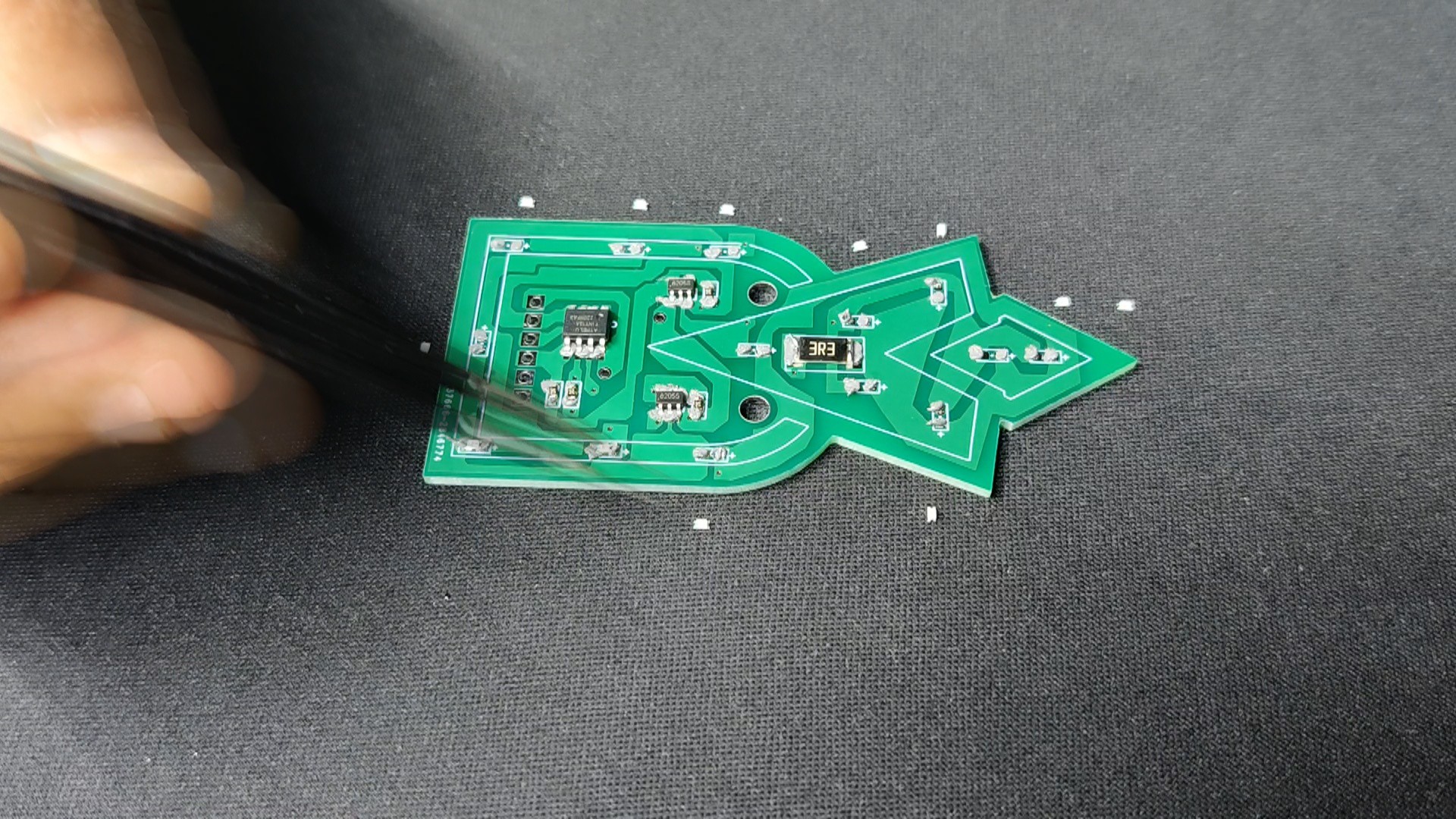
We started the PCB assembly process by applying solder paste to each component pad using a solder paste dispenser.
Next, we use an ESD Tweezer to pick and position each component one at a time in its proper location.
After that, we set the board on the reflow hotplate, which increases the temperature of the PCB from below to the point at which the solder paste melts. At that point, all of the components are connected to their pads.
We use a multimeter in diode checking mode, to check if the LEDs are connected to their pads correctly. We connect the positive probe to the LED's anode and the negative probe to the LED's cathode. This causes all of the LEDs that are connected in parallel to light up, indicating that the connections are correct.
2
CODE: Arduino as ISP
We are utilizing one of our earlier Arduino as ISP programmer to flash the Attiny13A. This programmer uses an Arduino Nano to flash a variety of AVR devices, including Atmega chips and Attiny.
you can checkout More about the Programmer from here:
In this case, we correctly connected the CON6 terminals of the ISP programmer and the Skyrim Quest marker.
We then choose attiny13A from the board manager and set the B.O.D to 1.5V along with choosing the Programmer to Arduino as ISP.
We press the burn the bootloader button, and this process will take 10-15 seconds, and you will be greeted with an "avrdude done" message.
Next, we open our sketch we want to upload, then go to the sketch menu and select upload using the programmer.
Our Sketch is now uploaded into the Attiny13A Microcontroller.
3
LAYER Assembly Process
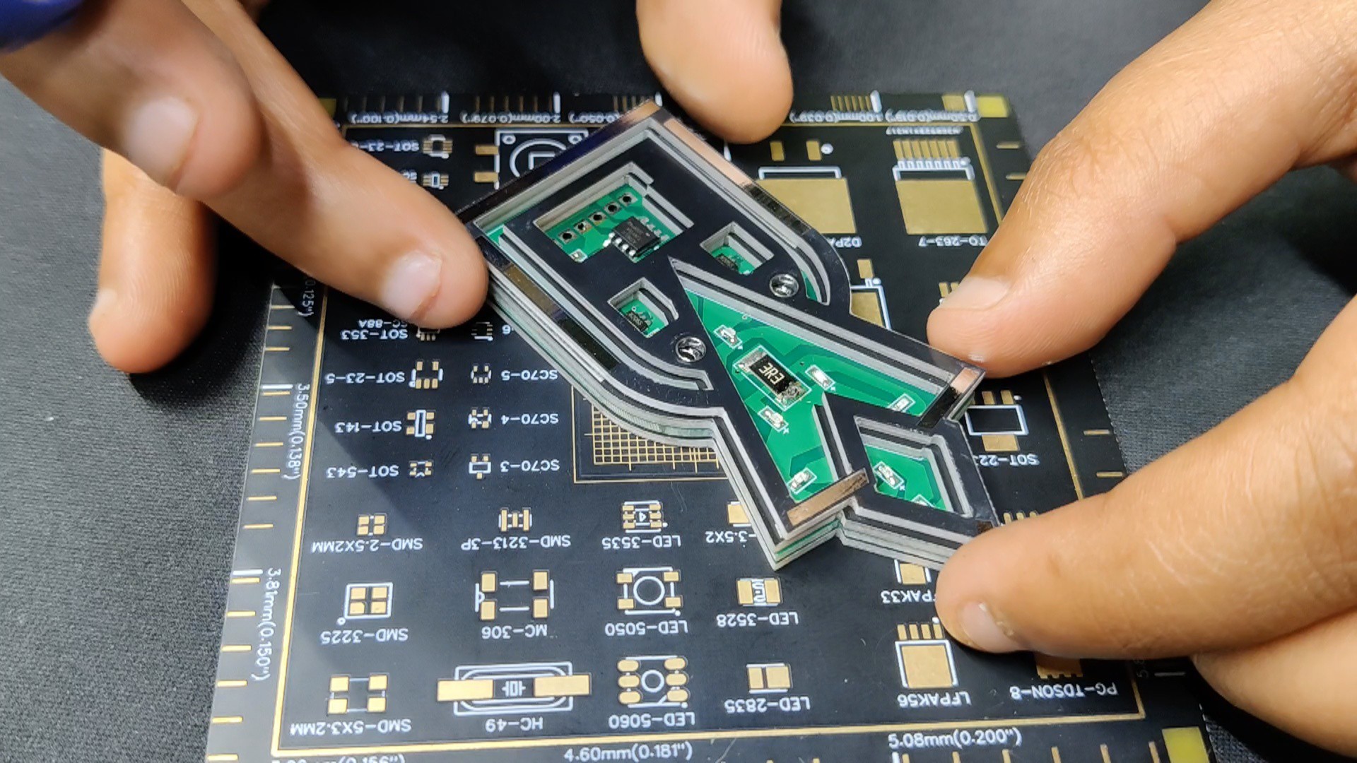
The layer assembly process now starts, with the bottom layer board being positioned on top of the middle layer board and another middle layer board being positioned on top of the bottom layer board.
Then, using a soldering iron to melt solder wire inside the mounting holes to fuse three layers together, this sandwich layer is put together.
We added another mid layer to the top side of the setup to give it a slight height so that the LEDs would diffuse properly. We then used solder wire to lock it in place on the mounting holes. Our current thick sandwitch PCB setup is made up of three separation layers, which make up the mid layer, and an electrical layer, which is the bottom layer.
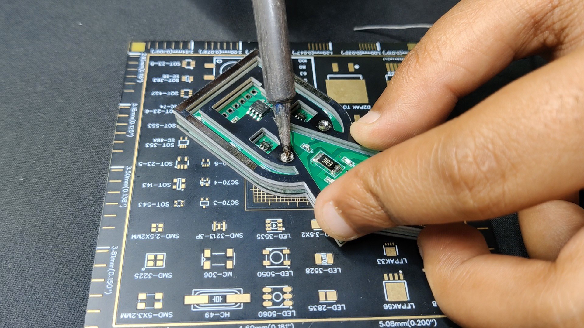
The top layer was then added, and it was positioned using the mounting holes. We used a soldering iron and solder wire to attach the top layer to the other layers, securing them in place.
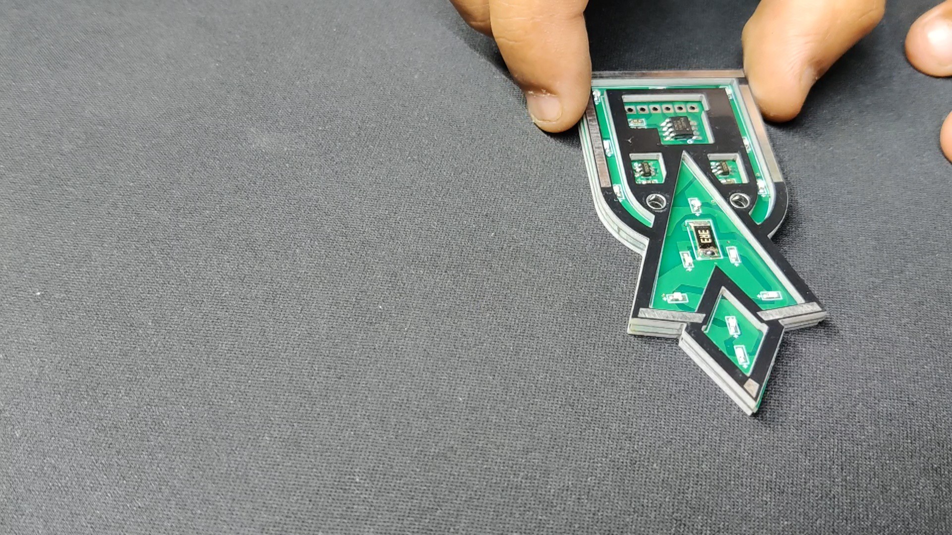
Assembly is now complete.
4
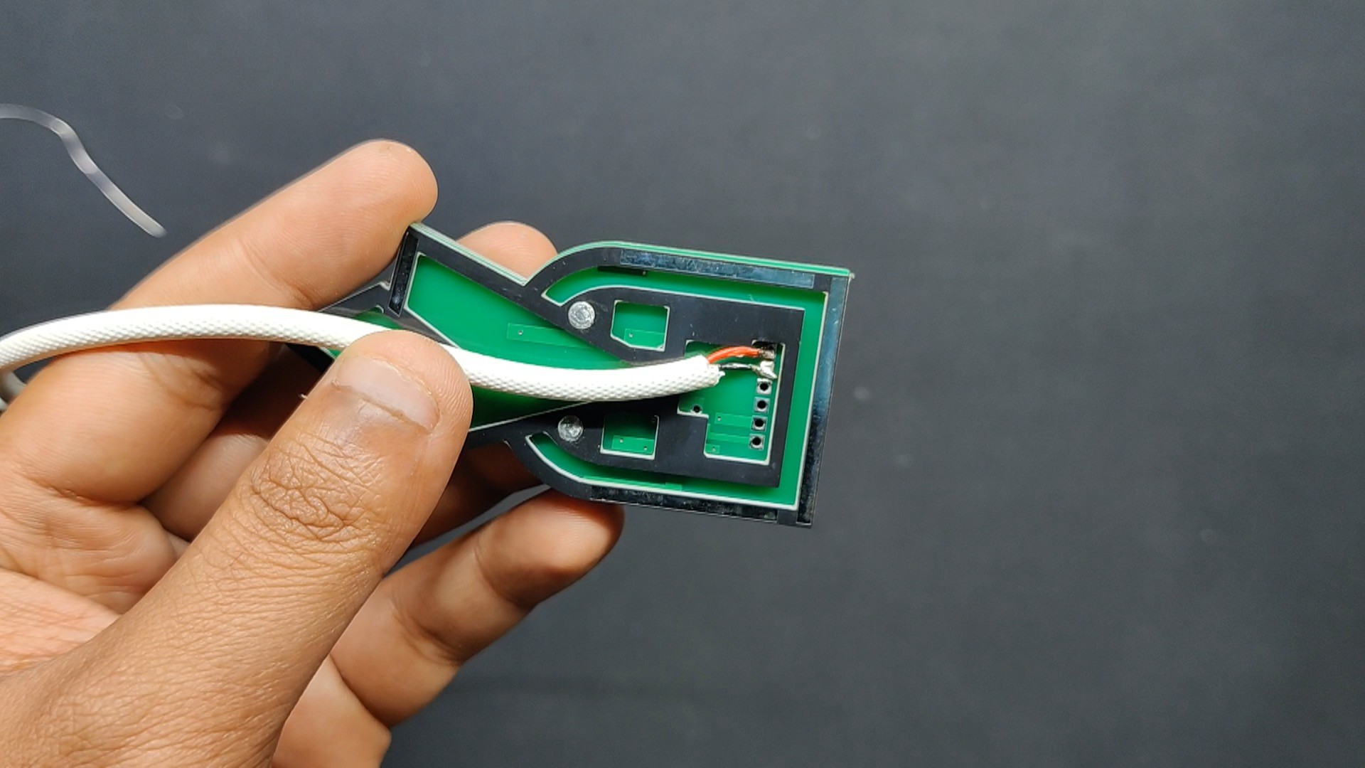
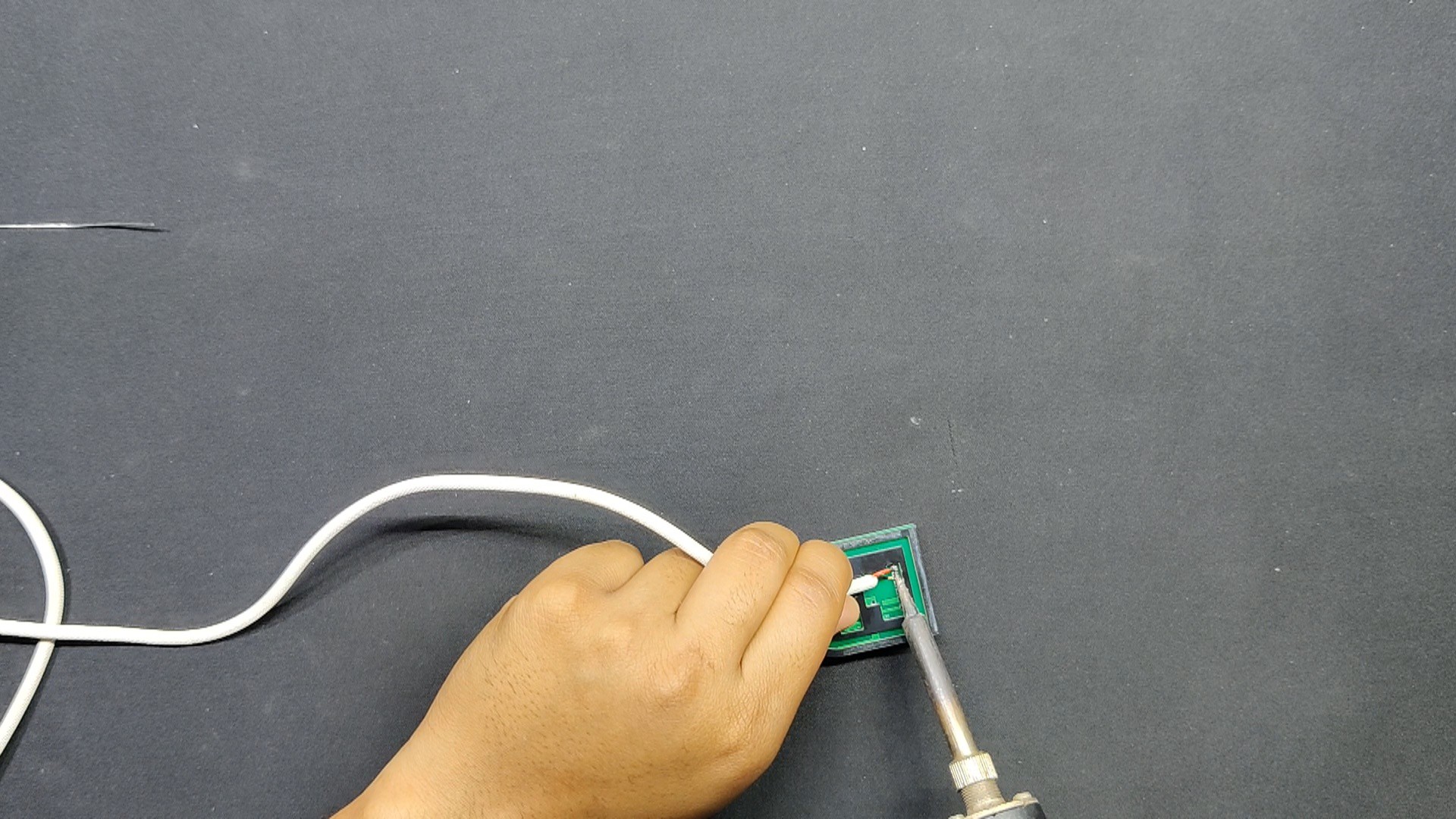
Power Source
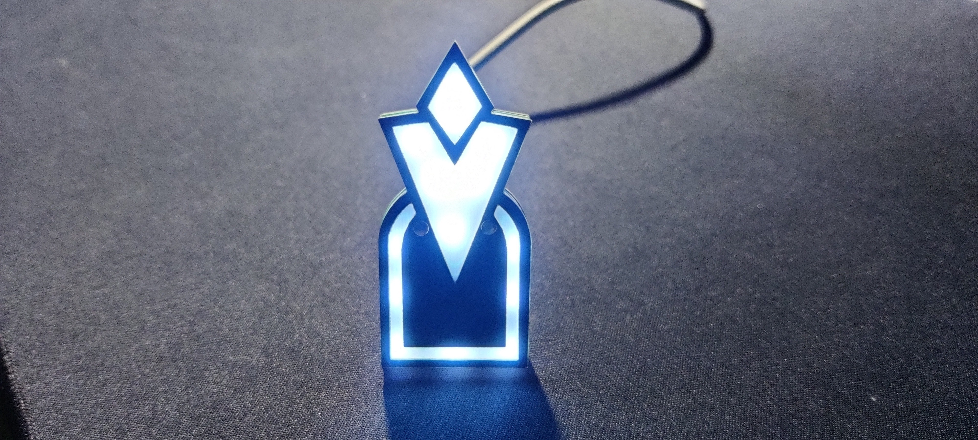
Following assembly, the board needed to be powered. To do this, we used a USB cable, cutting off the Micro USB end and attaching the positive and negative wires to the VCC and GND terminals on the CON6 terminal.
Our device will be powered on when the USB cable is inserted into any 5V USB socket.
5
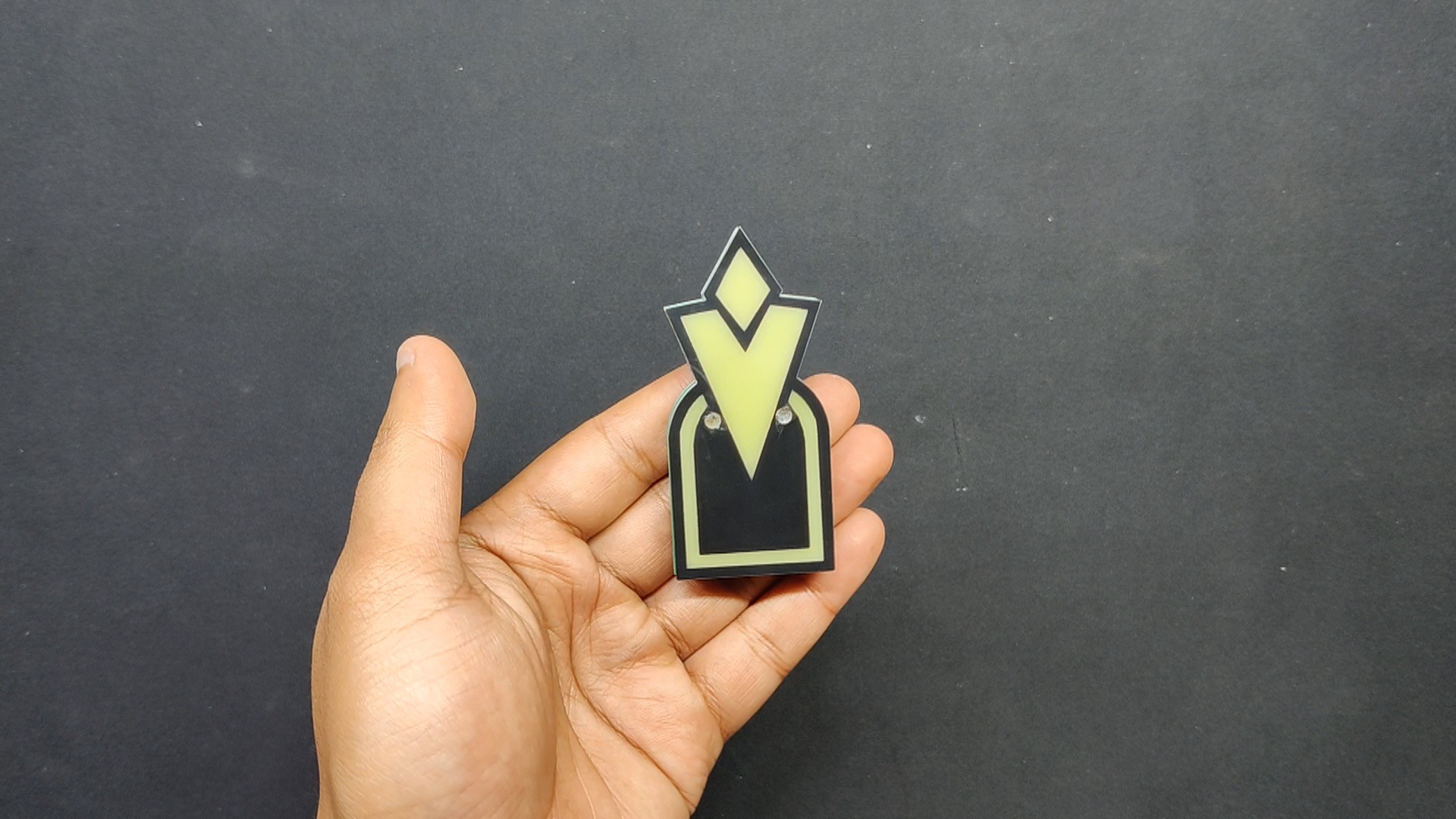
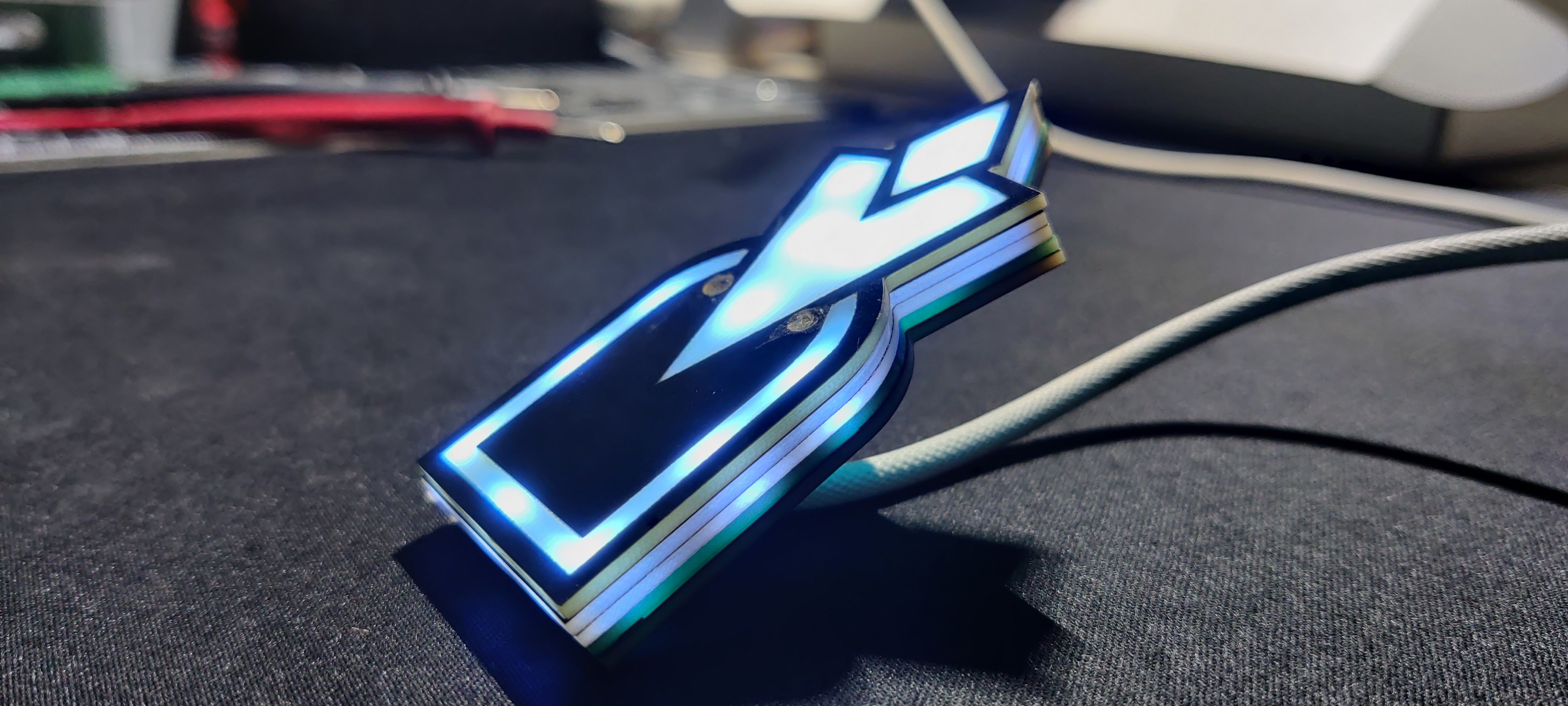
Result
This straightforward build resulted in a Skyrim Marker that resembles its in-game equivalent perfectly. The most fascinating aspect of this concept was how the entire thing was constructed out of PCBs, including the top layer that diffuses the light from the LEDs, the separating layer that adds height to the structure, and the mainboard that houses all the components.
I wanted to push myself by building something that requires PCBs, but not just for electrical connections. This project could have been easily constructed with a 3D printed body, but it would have been extremely simple. This approach's concept originated with the Geek Club PCB kits.
Overall this project was completed and needed no further revisions.
Special thanks to HQ NextPCB for providing components that I've used in this project, check them out for getting all sorts of PCB or PCBA-related services for less cost.
Thanks for reaching this far, and I will be back with a new project soon.
 Arnov Sharma


Discussions
Become a Hackaday.io Member
Create an account to leave a comment. Already have an account? Log In.