Arnov Sharma
Design
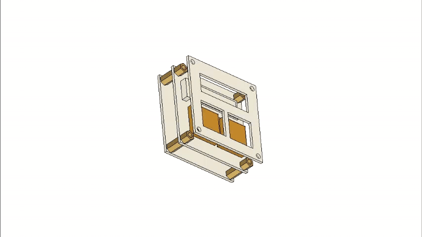
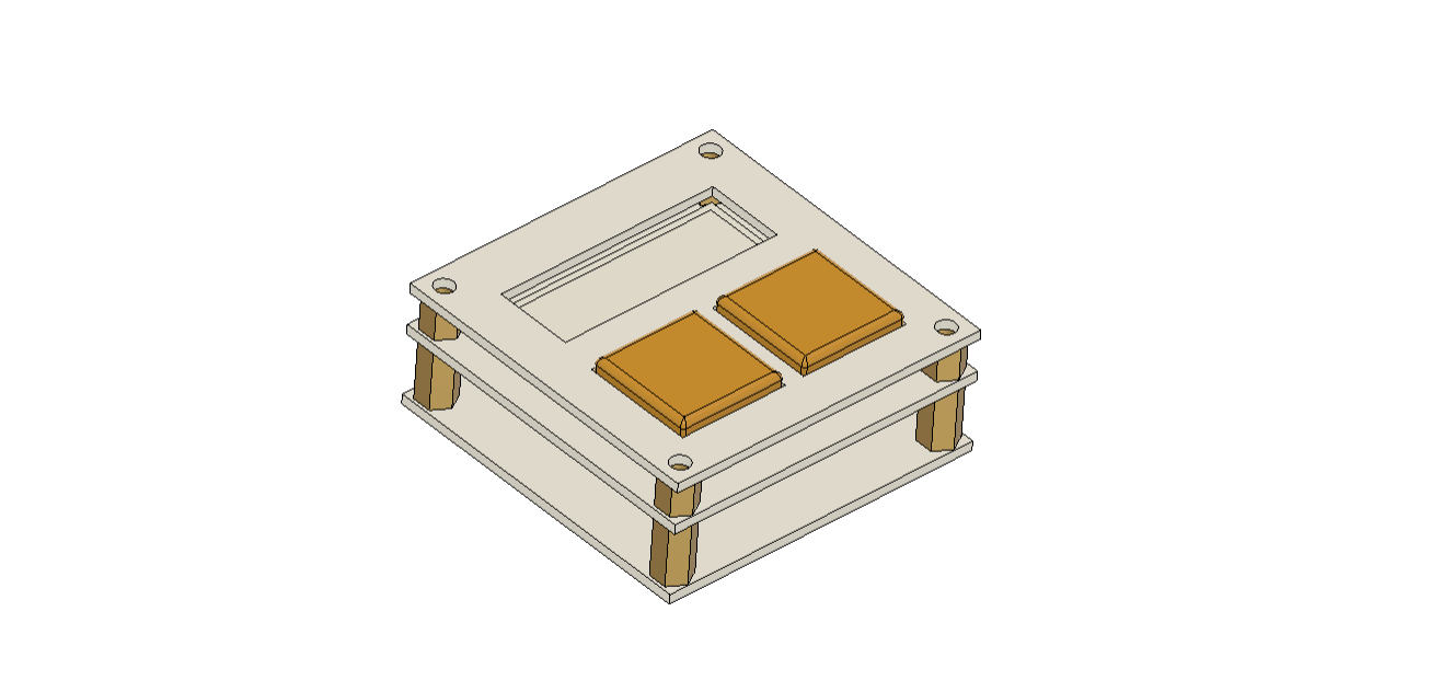
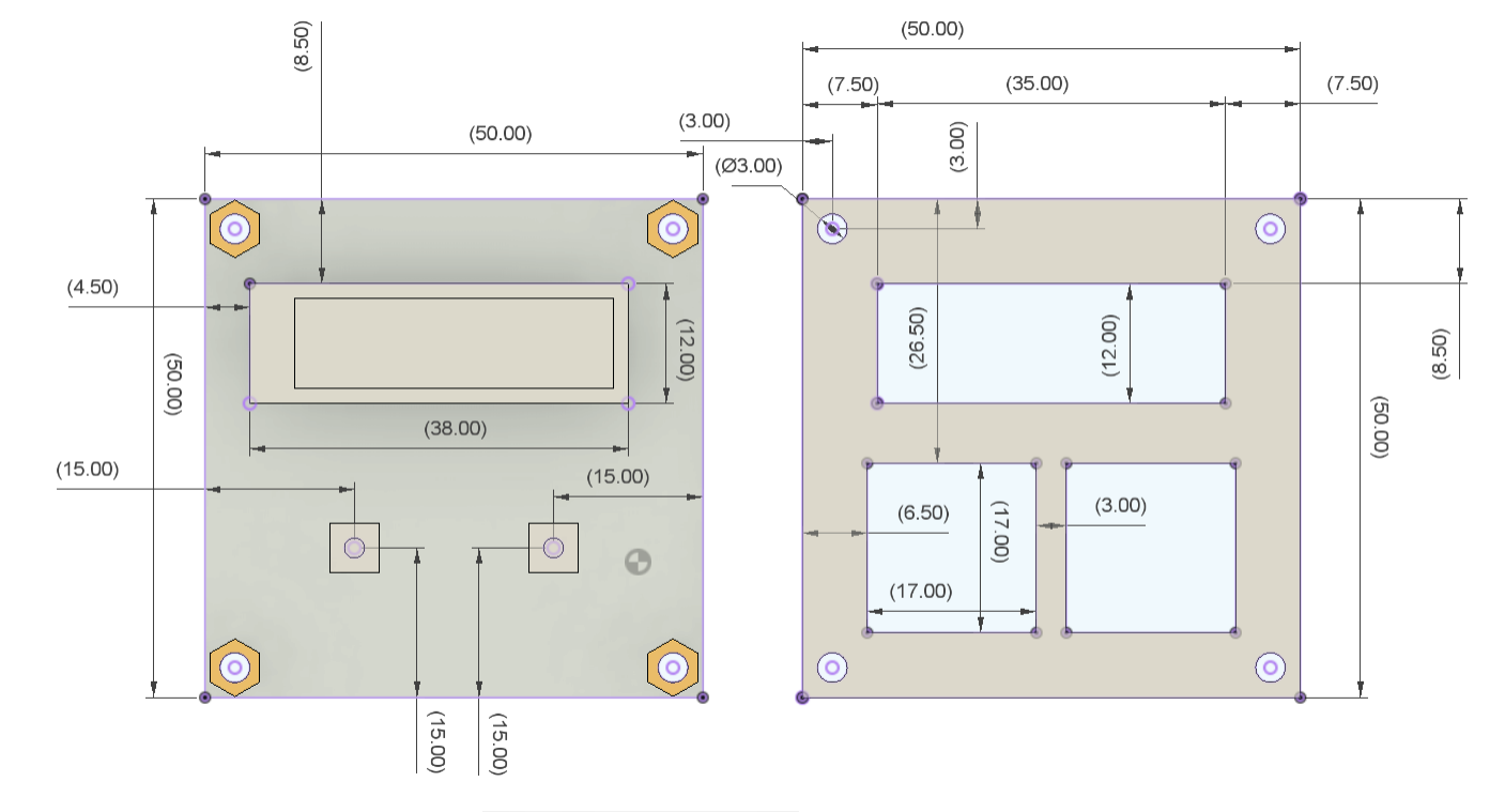
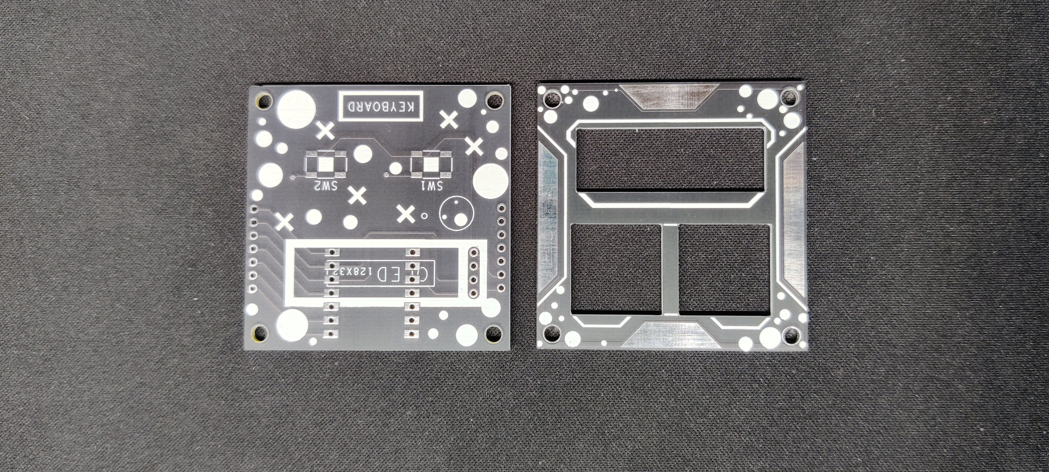
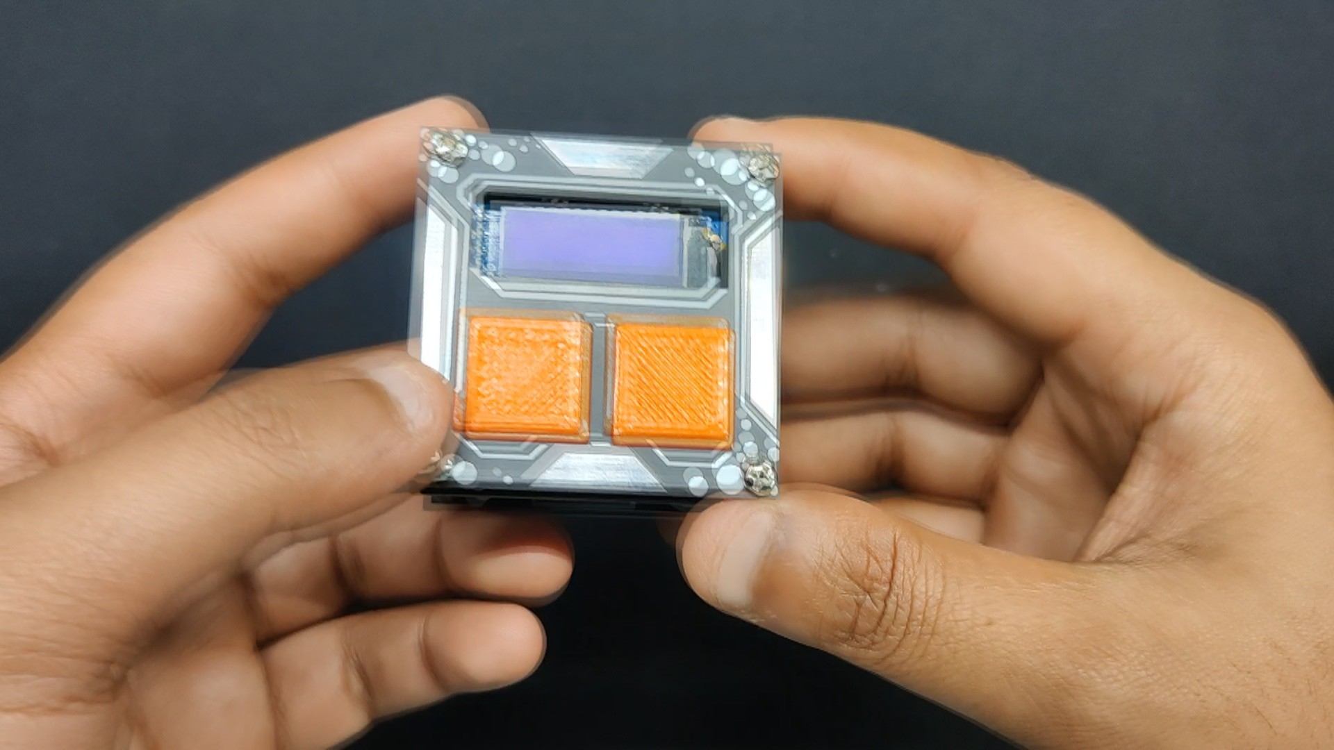
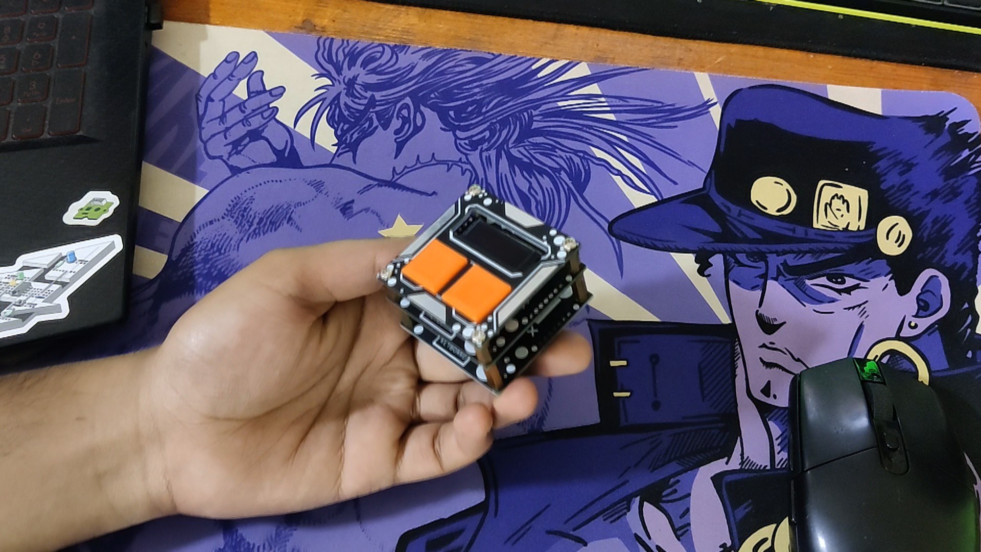
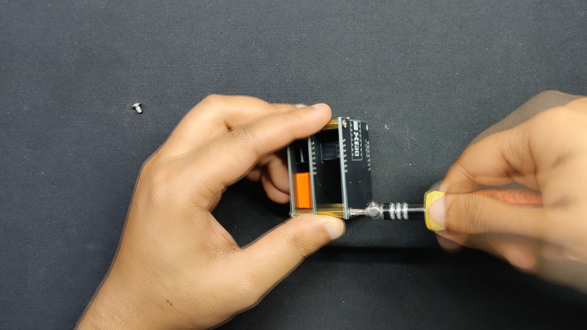
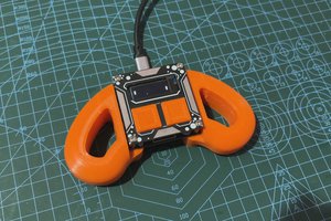
In the beginning, we built the PastPal model utilizing three PCB layers stacked together with eight PCB STANDOFFS: four for connecting the top layer to the mid layer and another four for connecting the mid layer to the base layer.
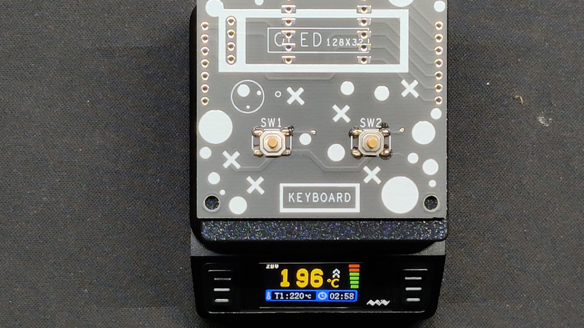
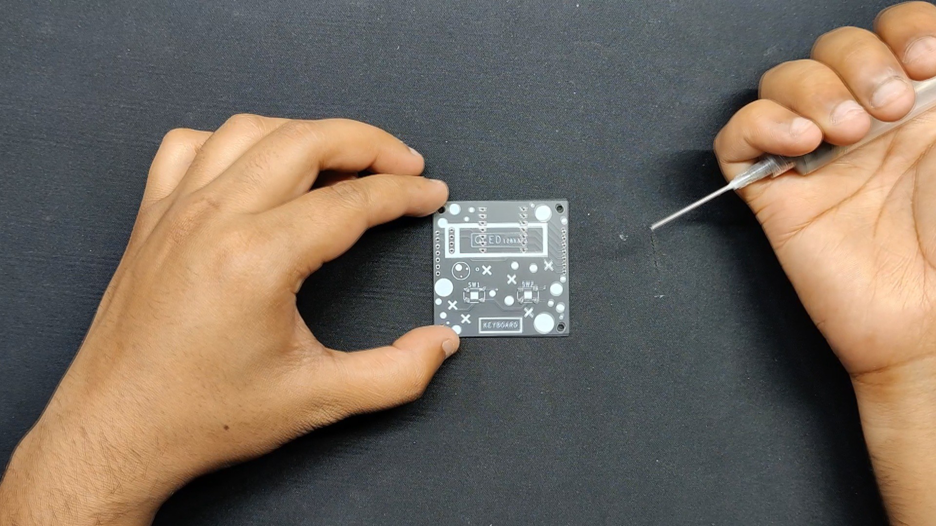
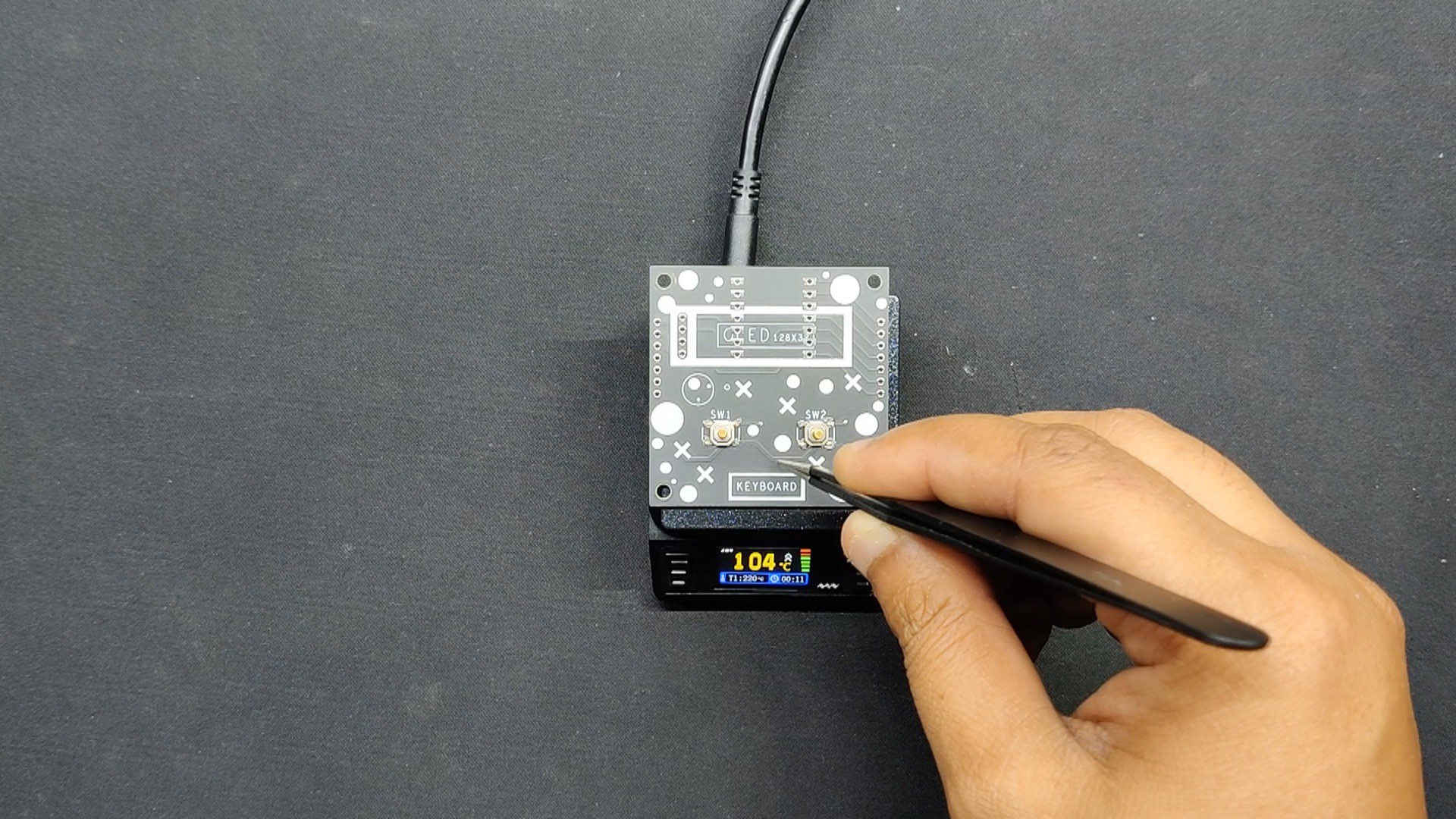
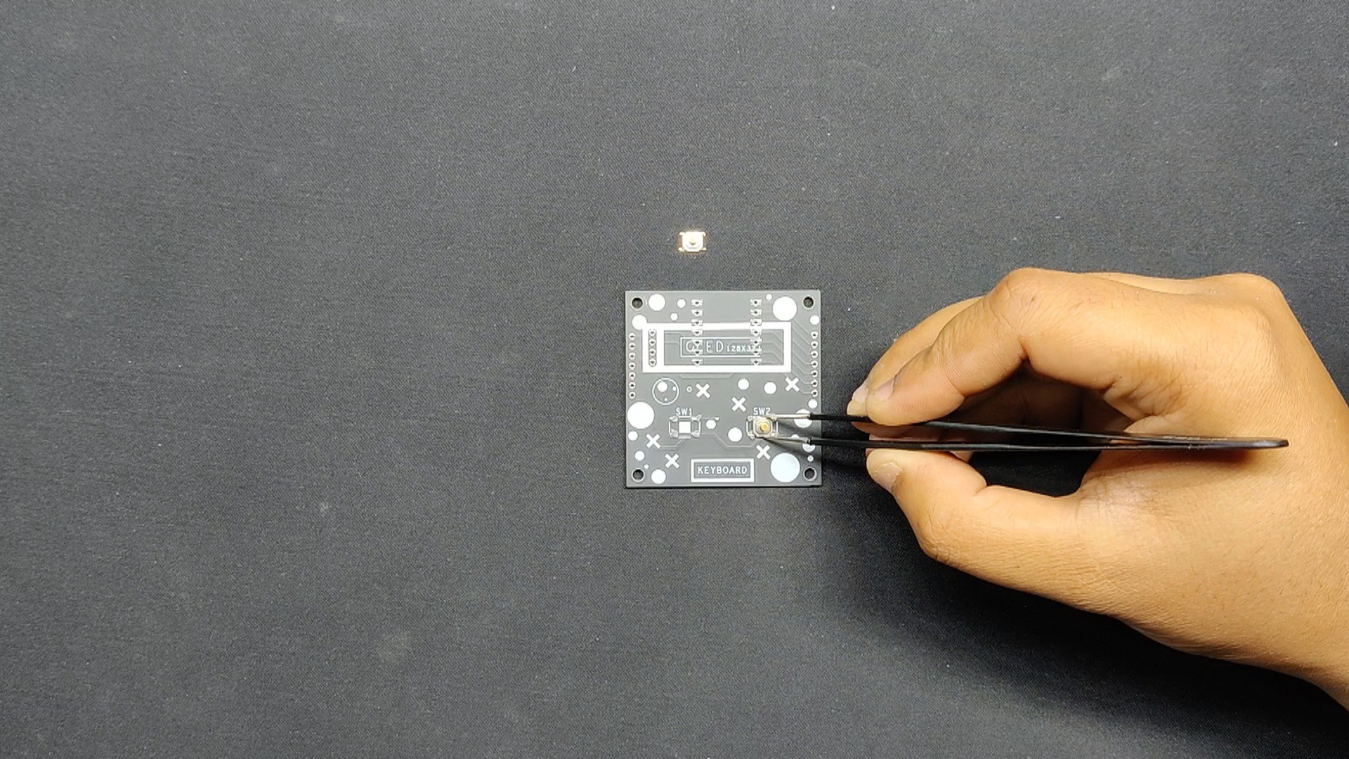
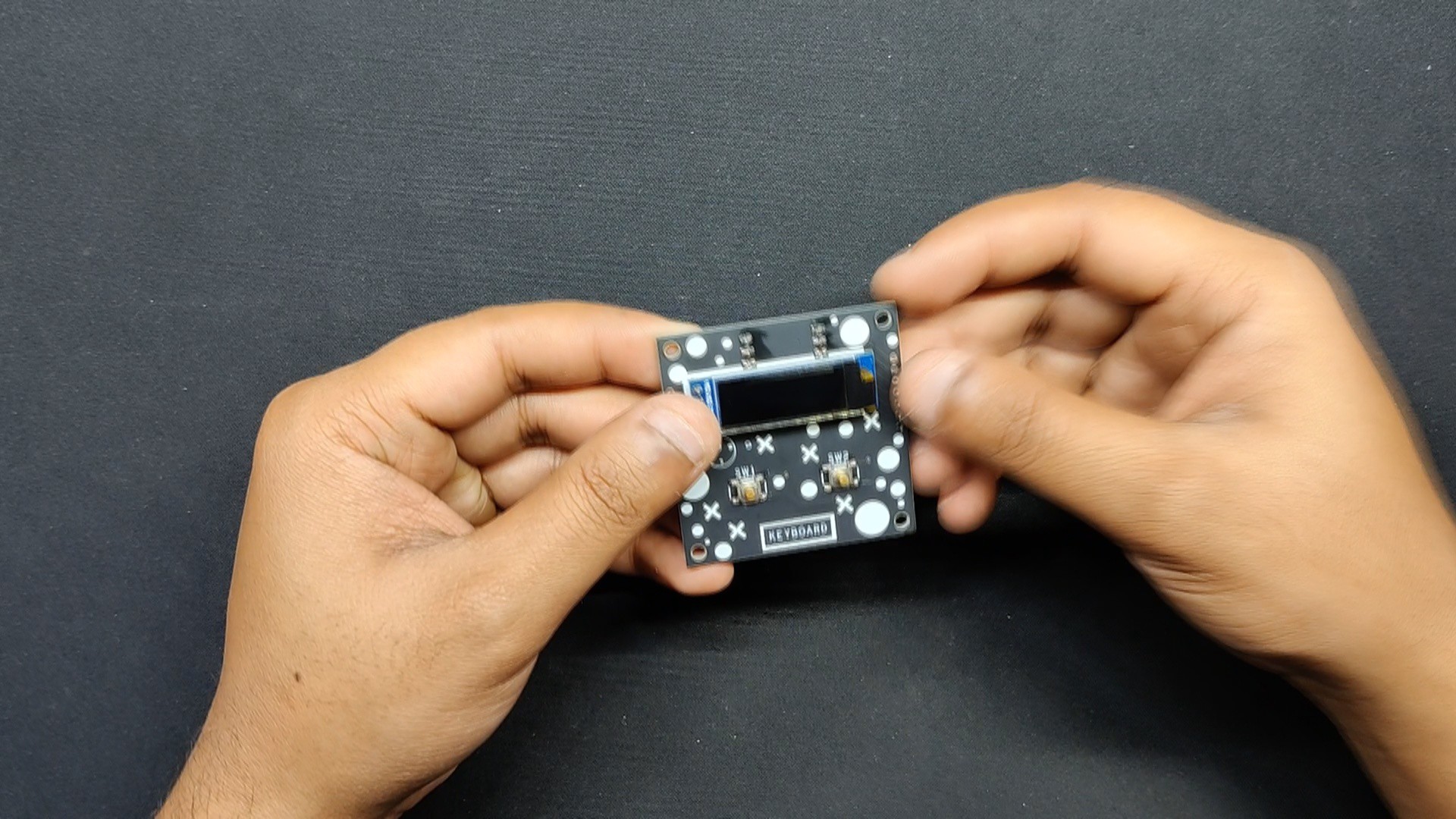
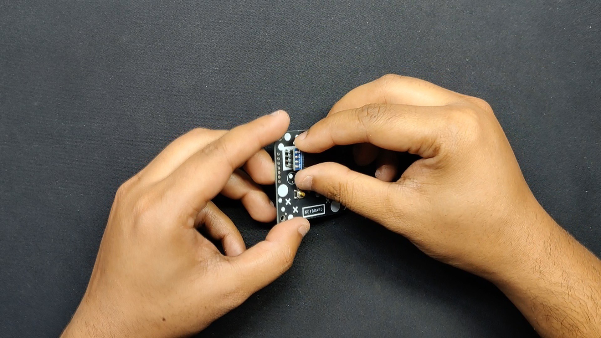
Three openings have been made on the top layer: two are for the addition of the switch actuator, and one is for the display.
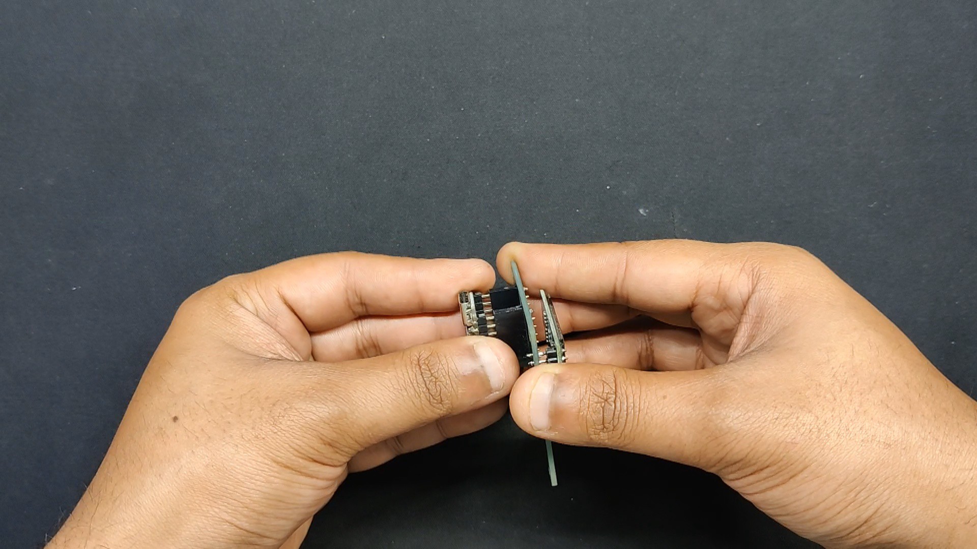
The mid layer has an XIAO microcontroller on the bottom face of the board and SMD switches and a display on the top face.
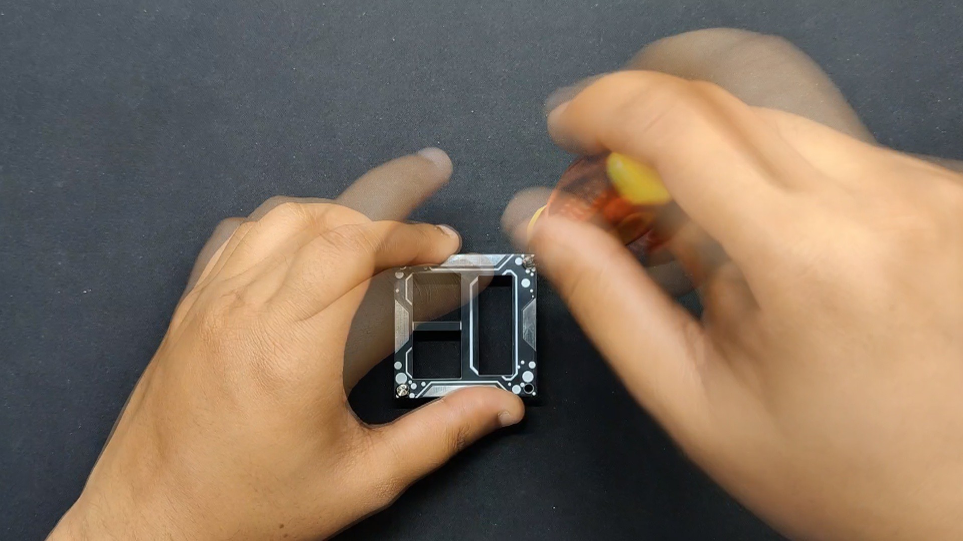
To enclose the model from the bottom, there is a third layer dubbed the bottom layer.
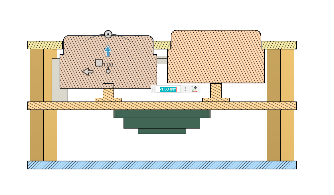
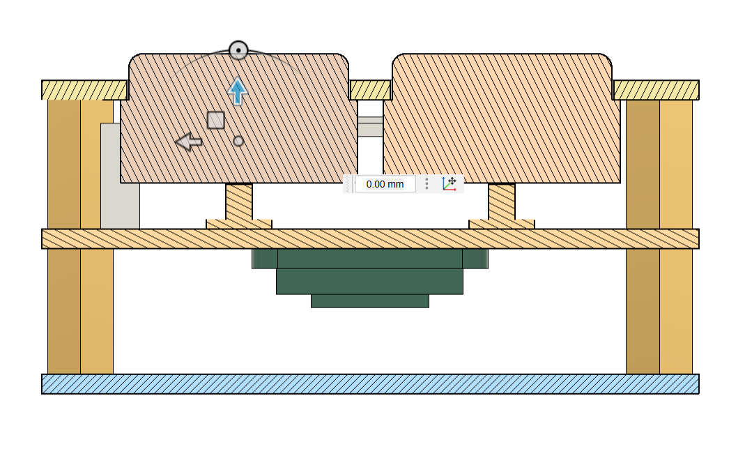
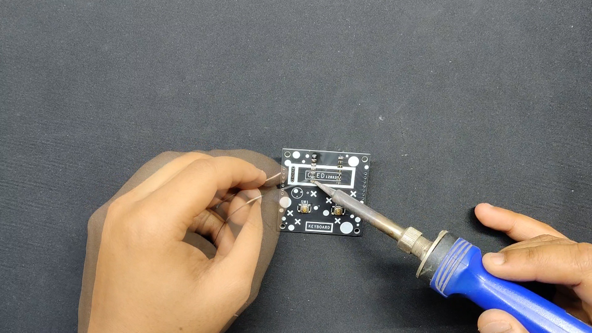
The switch actuators are modeled and positioned between the switch actuator slots on the top layer and on top of the SMD switch knob.
Since the switch actuator and the switch knob are positioned exactly on top of one another, pressing the switch actuator also presses the knob, resulting in a registered switch click.
PCB Design
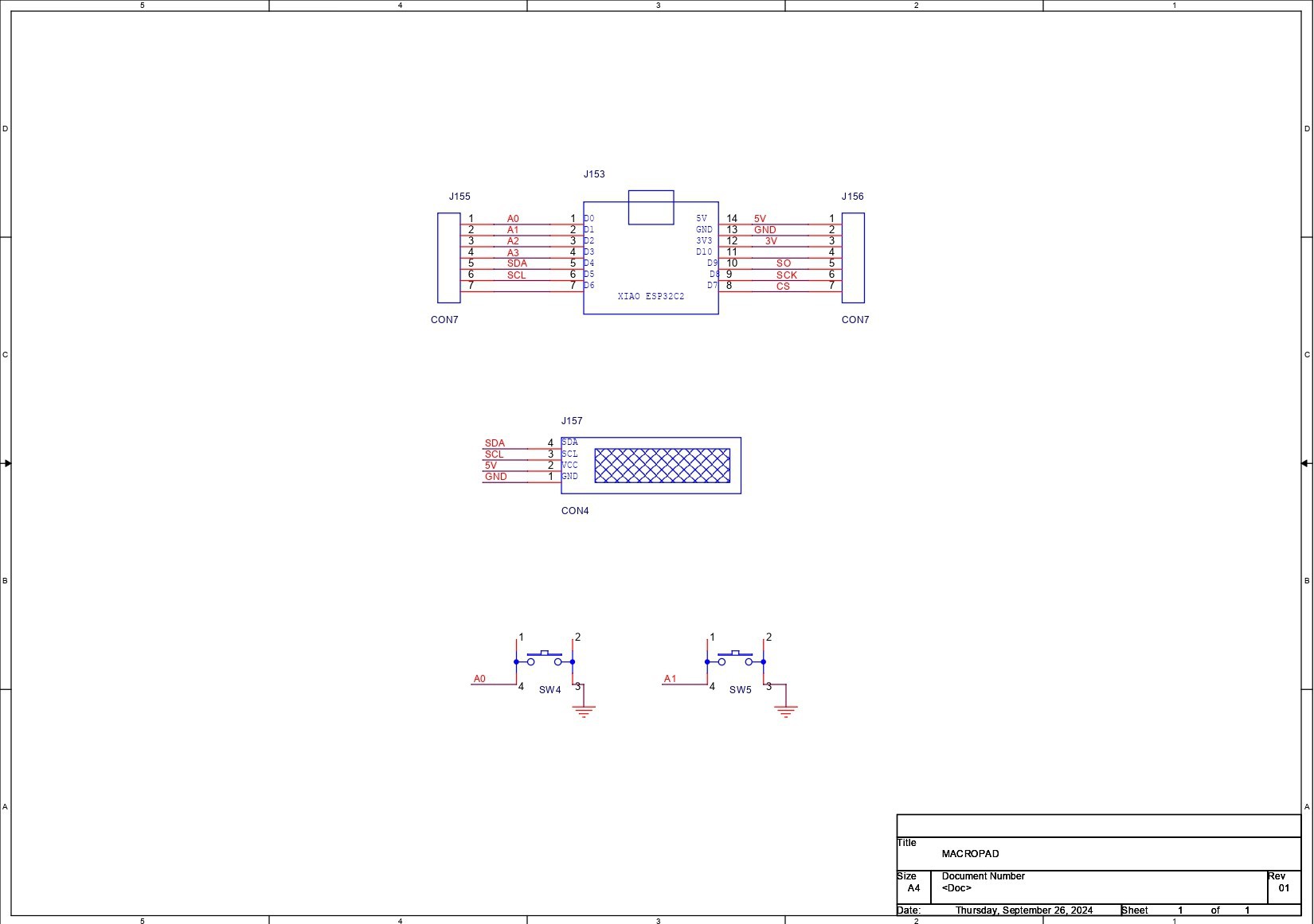
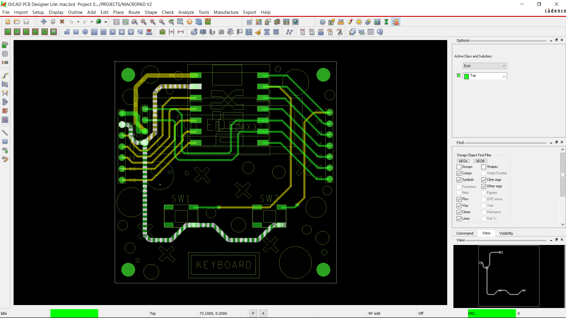
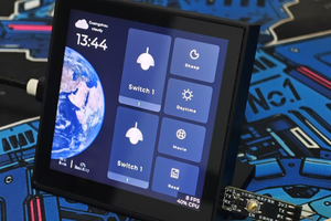
The PCB design for this project was quite easy to interpret; we included an XIAO SAMD21 Microcontroller, whose D0 and D1 I/O Pins are used to connect it to two SMD switches. Additionally, we integrated an OLED display using XIAO's I2C Pins.
Since the SAMD21 microcontroller inside the XIAO is registered as a human interface device (HID), we can create a tiny two-switch keyboard using the Arduino keyboard library.
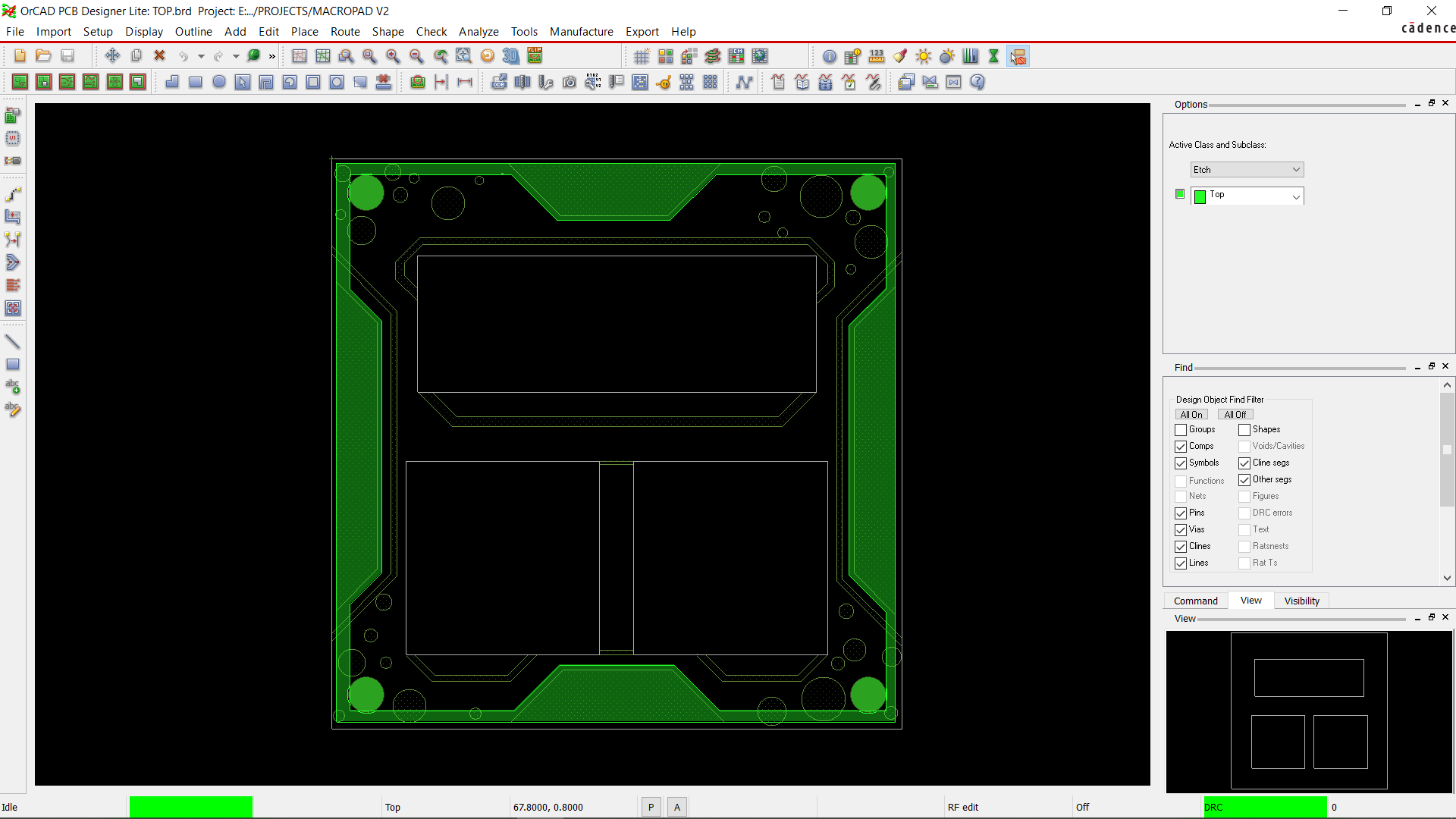
We made two boards using the model's dimensions: the top layer board and the mid layer board. Since the mid layer board and the bottom layer have the same outline and mounting holes, we will use it for the bottom layer.
HQ NextPCB Service
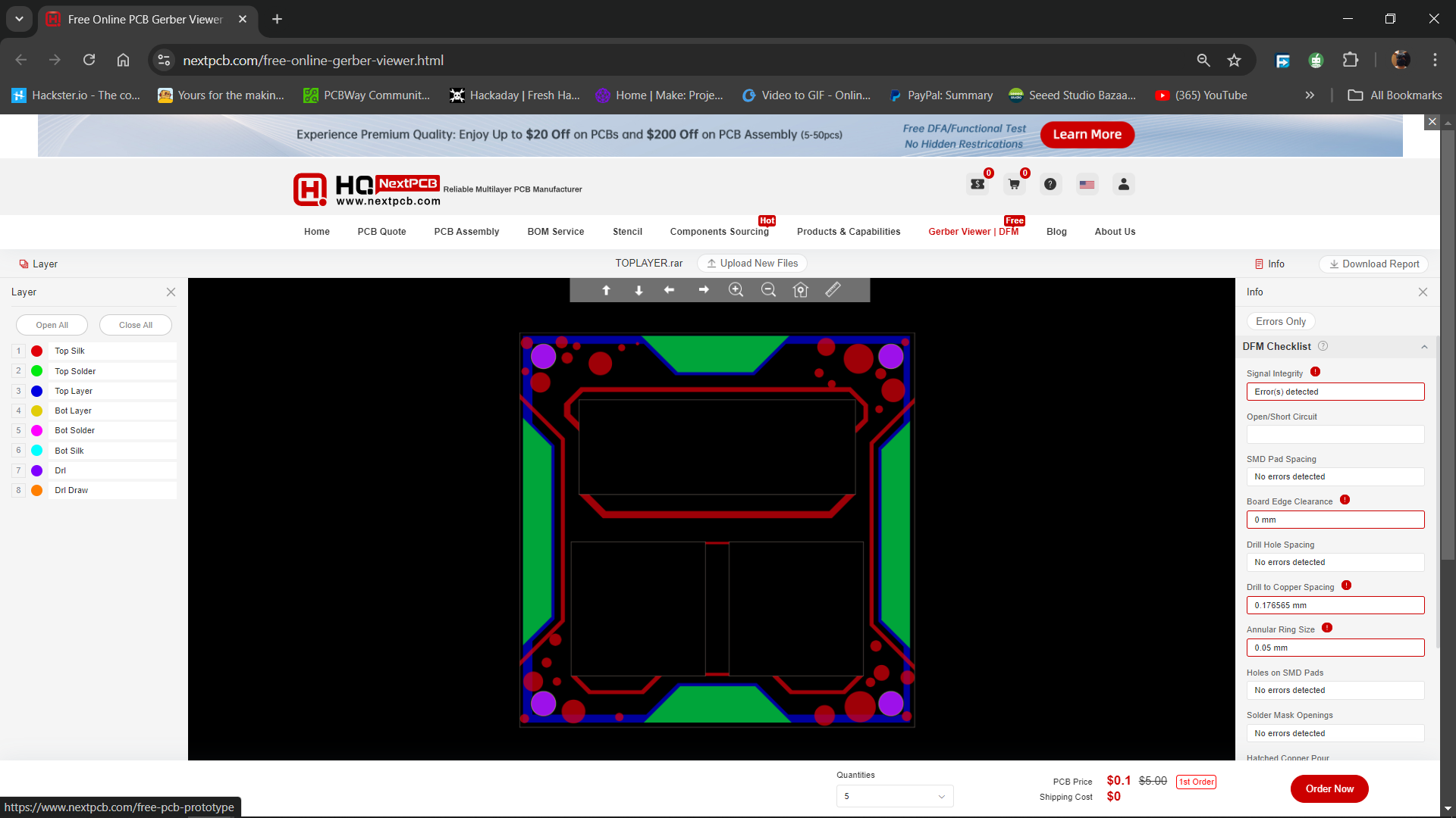
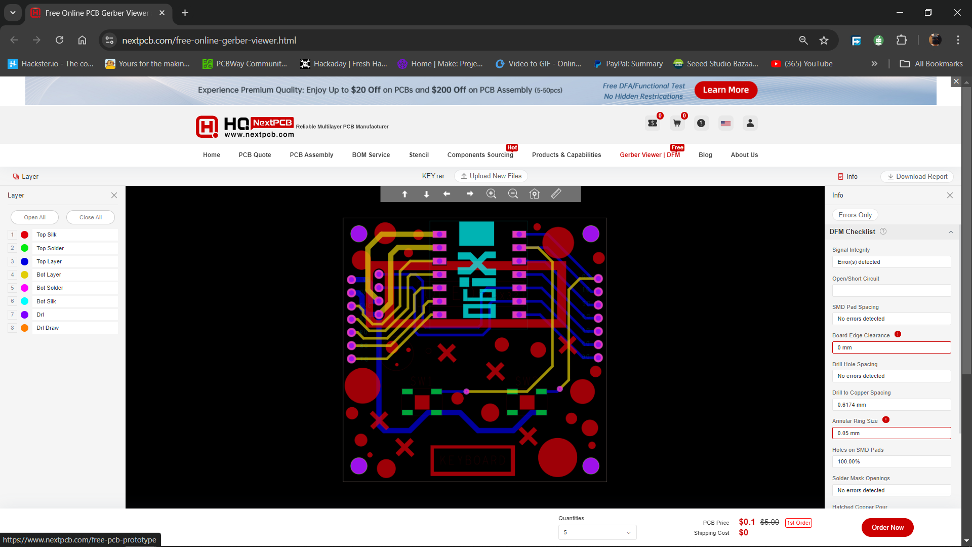
After completing the PCB design, we export the Gerber data and send it to HQ NextPCB for samples.
For the mid and top layer boards, two orders were placed. We ordered Black Solder mask with White Screen for the Mid and Top Layer Board.
After placing the order, the PCBs were received within a week, and the PCB quality was pretty great.
In addition, I have to bring in HQDFM to you, which helped me a lot through many projects. Huaqiu’s in-house engineers developed the free Design for Manufacturing software, HQDFM, revolutionizing how PCB designers visualize and verify their designs.
HQDFM: Free Online Gerber Viewer and DFM Analysis Tool
Also, NextPCB has its own Gerber Viewer and DFM analysis software.
Your designs are improved by their HQDFM software (DFM) services. Since I find it annoying to have to wait around for DFM reports from manufacturers, HQDFM is the most efficient method for performing a pre-event self-check.
Here is what online Gerber Viewer shows me. Would not be more clear. However, for full function, like DFM analysis for PCBA, you, need to download the software. The online version only provides a simple PCB DFM report.
With comprehensive Design for Manufacture (DFM) analysis features, HQDFM is a free, sophisticated online PCB Gerber file viewer.
It provides insights into advanced manufacturing by utilizing over 15 years of industry expertise. You guys can check out HQ NextPCB if you want great PCB service at an affordable rate.


 Ai-Thinker