Design idea
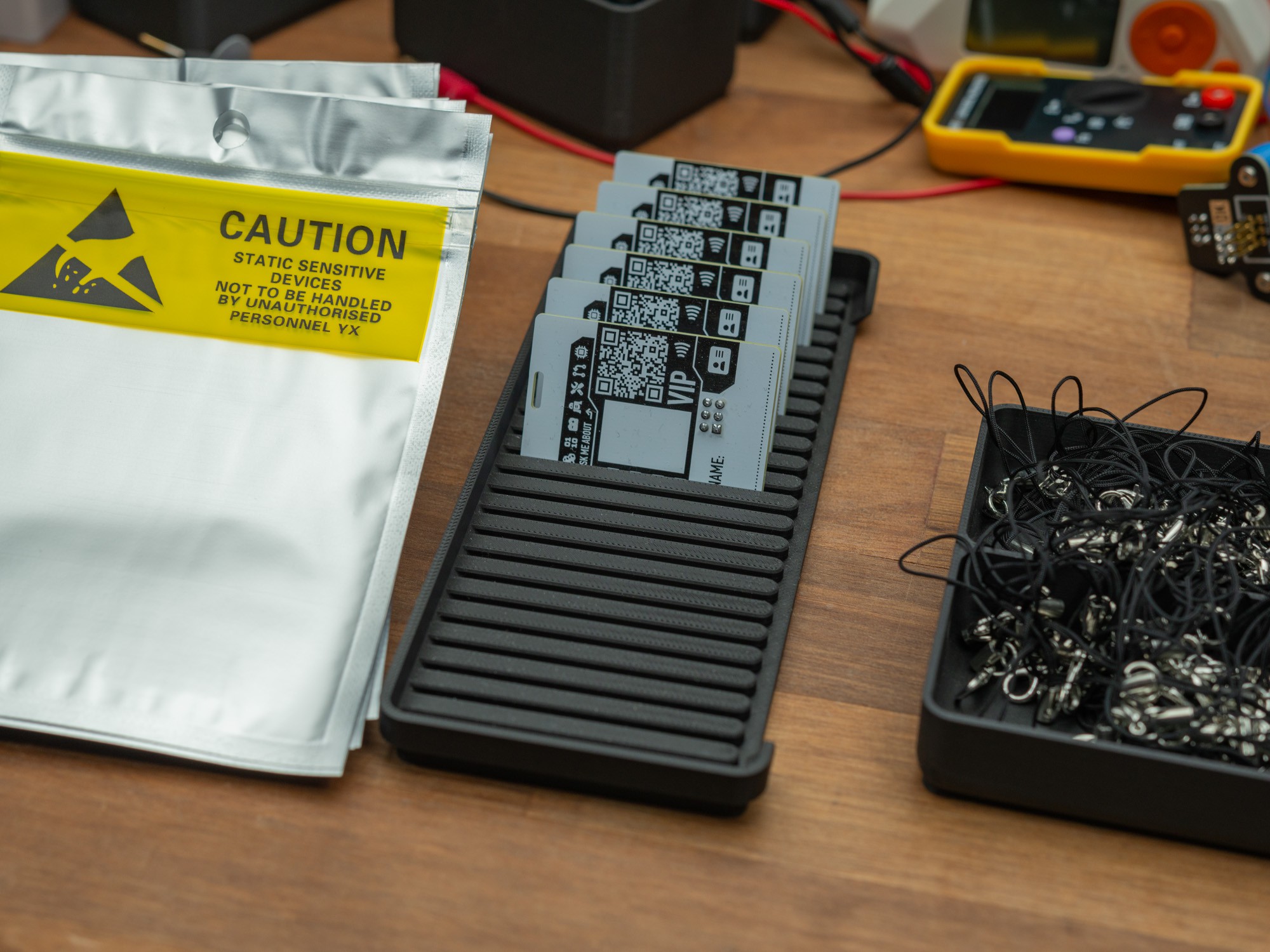
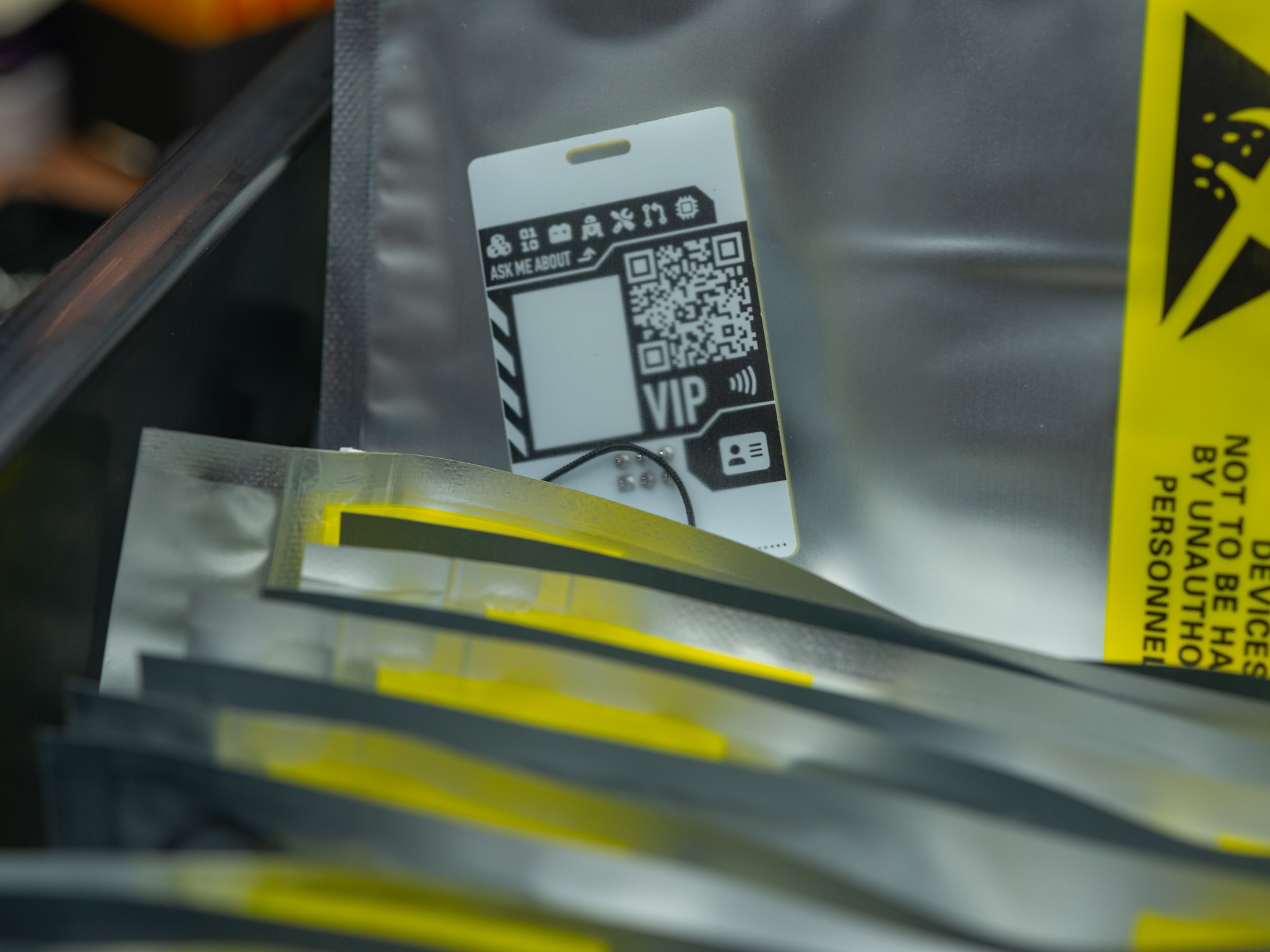
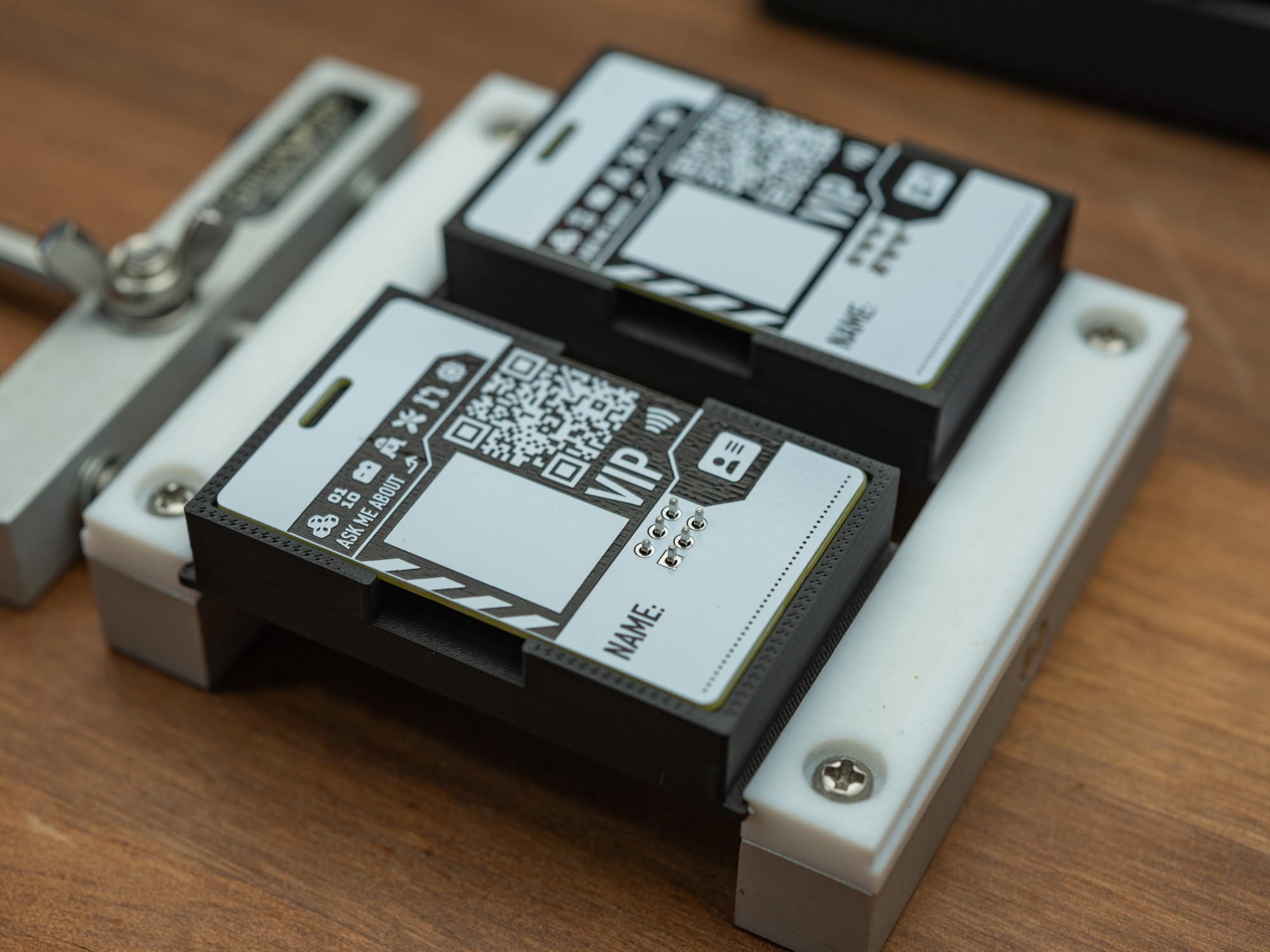
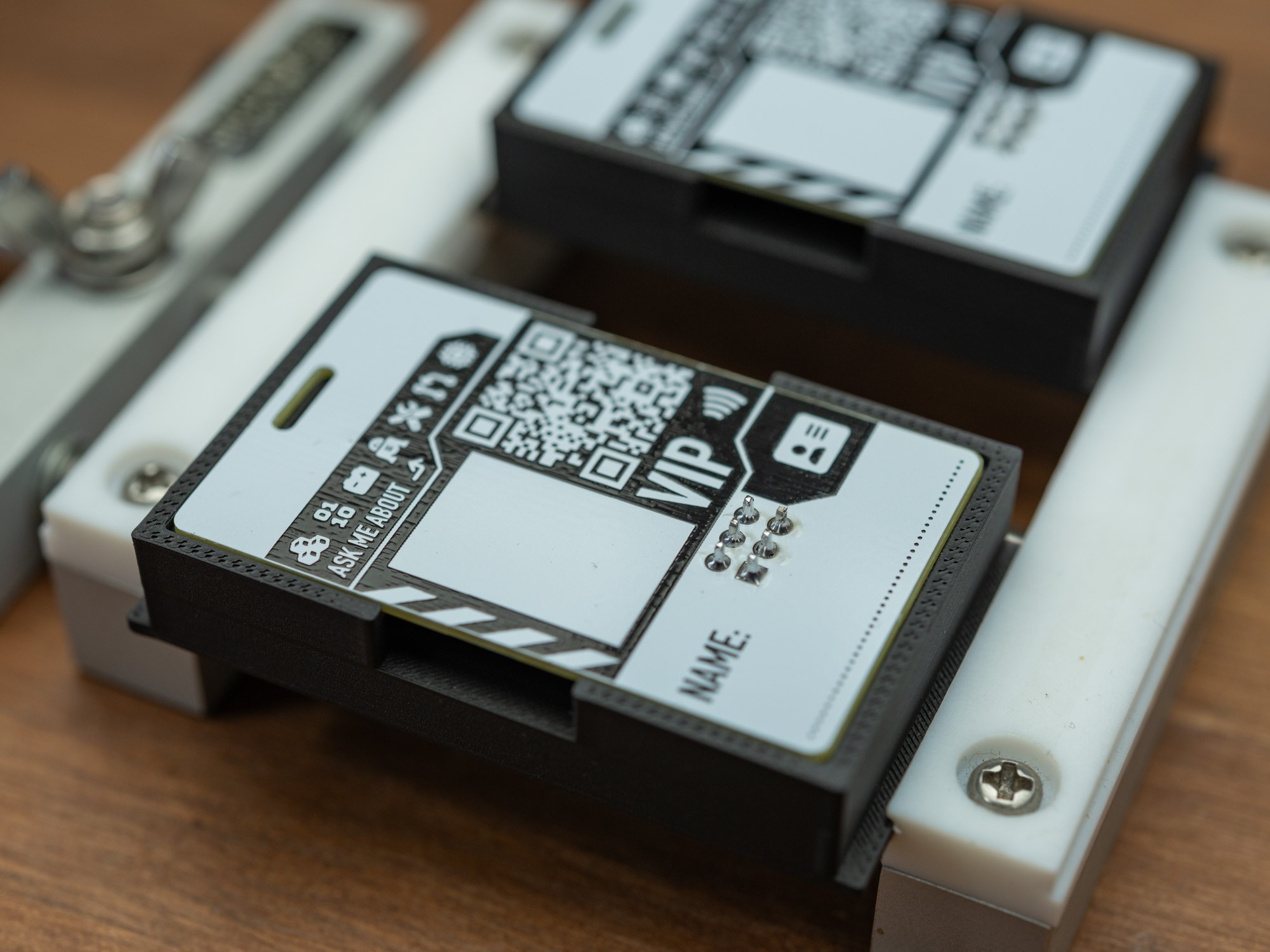
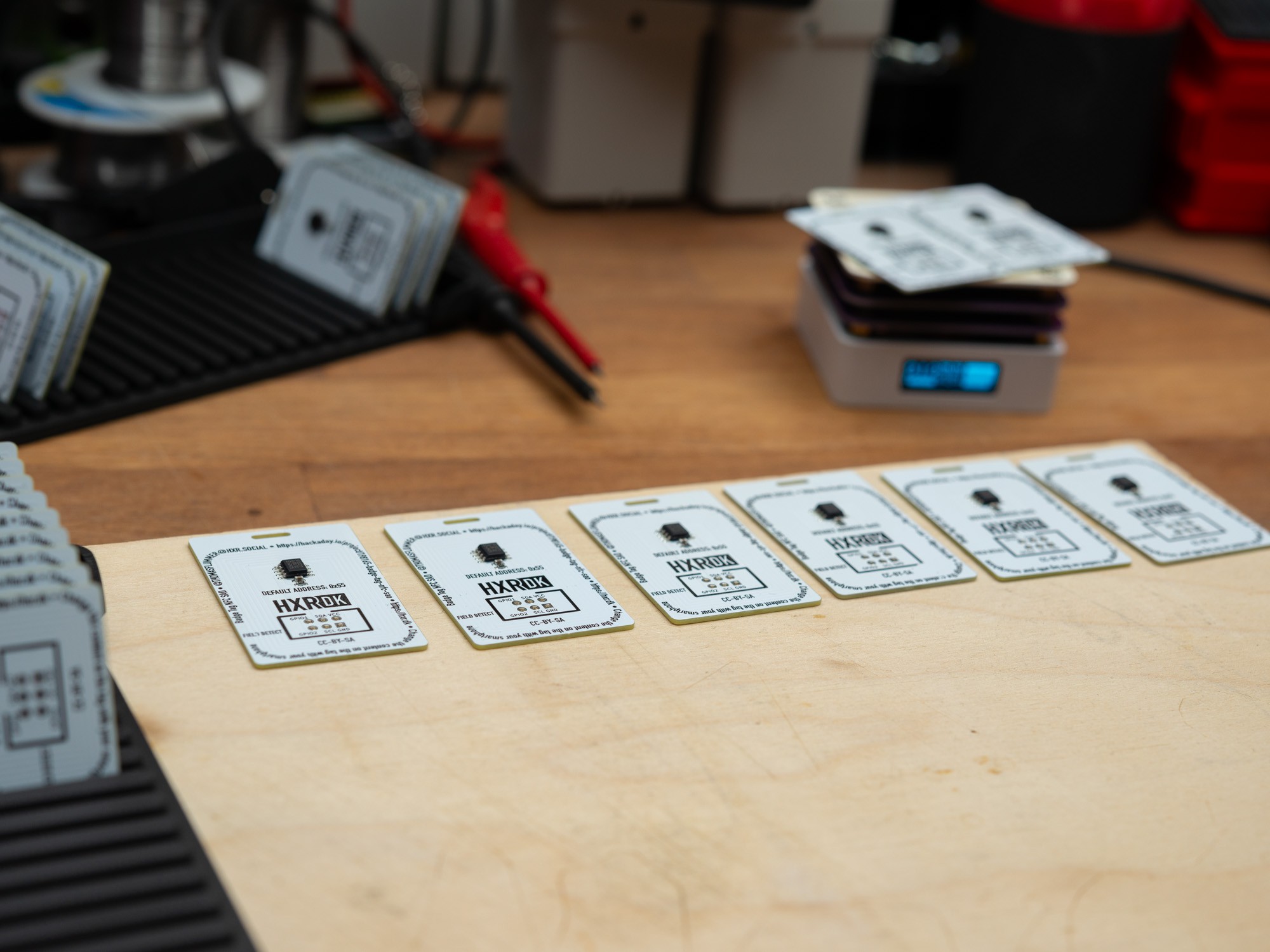
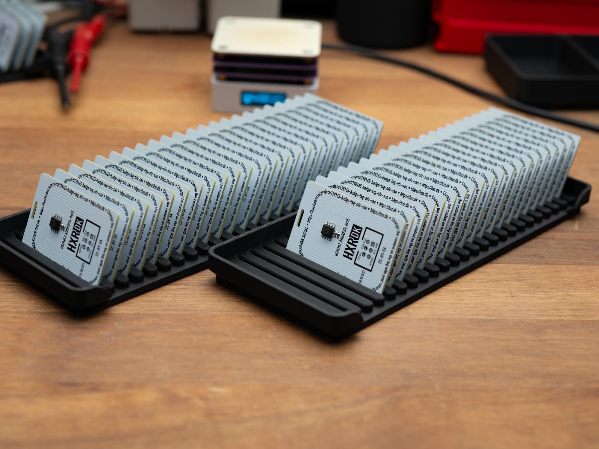
It's designed with the aim of mimicking a regular work or government access credential, and due to the NFC chip, it could potentially be enrolled and function in the same way.
Mechanical
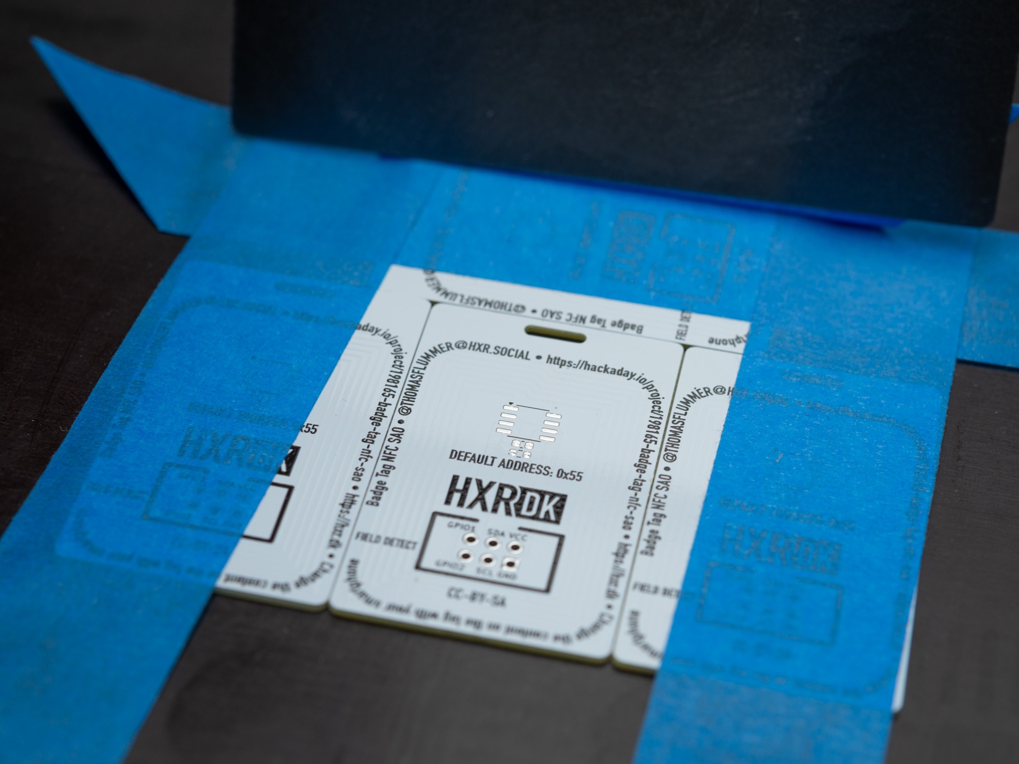
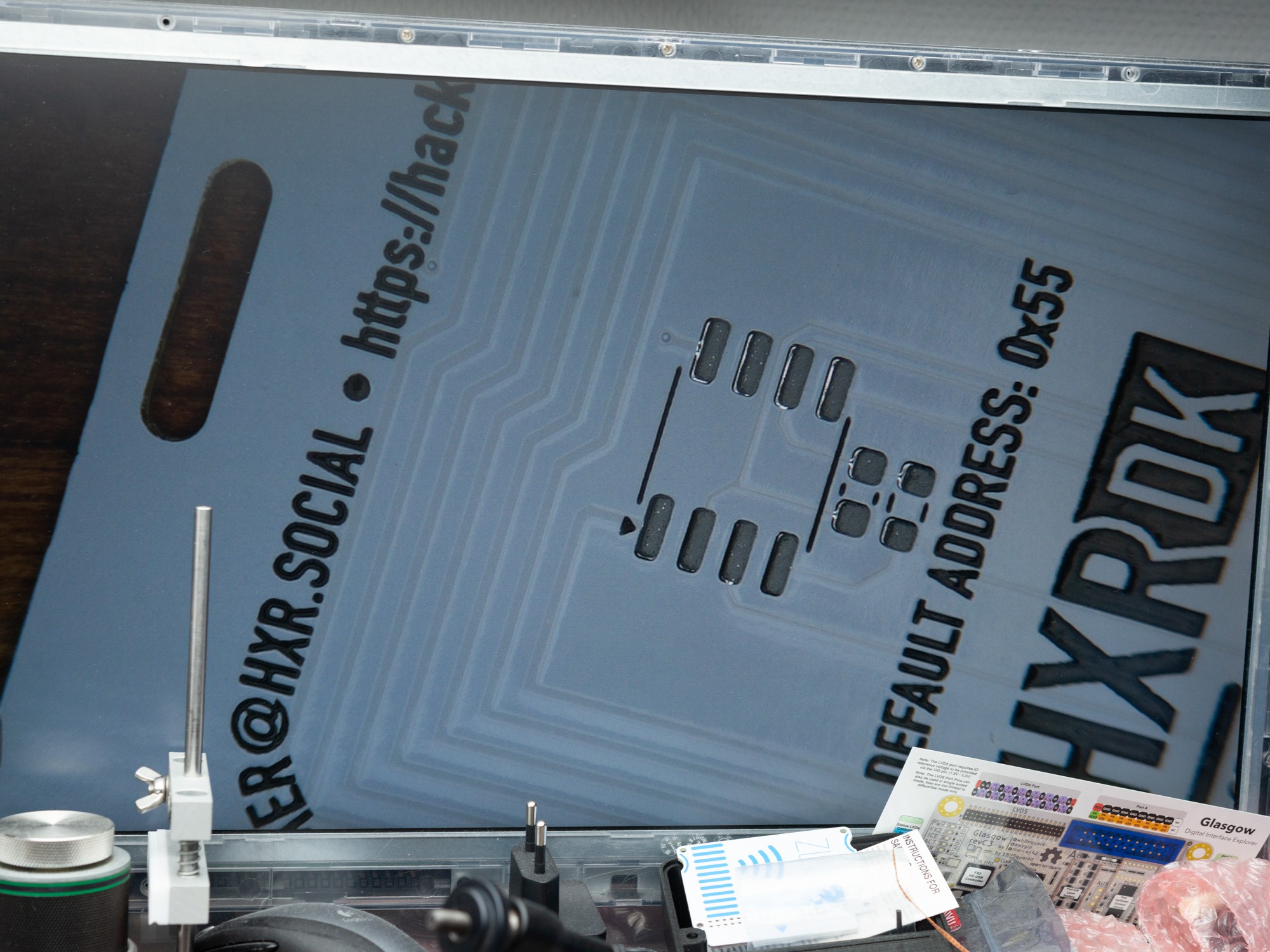
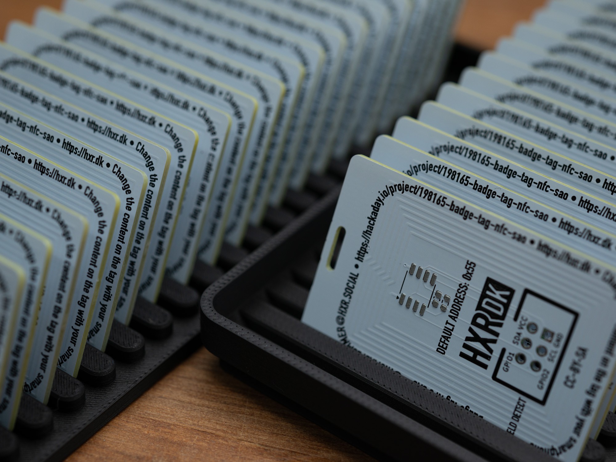
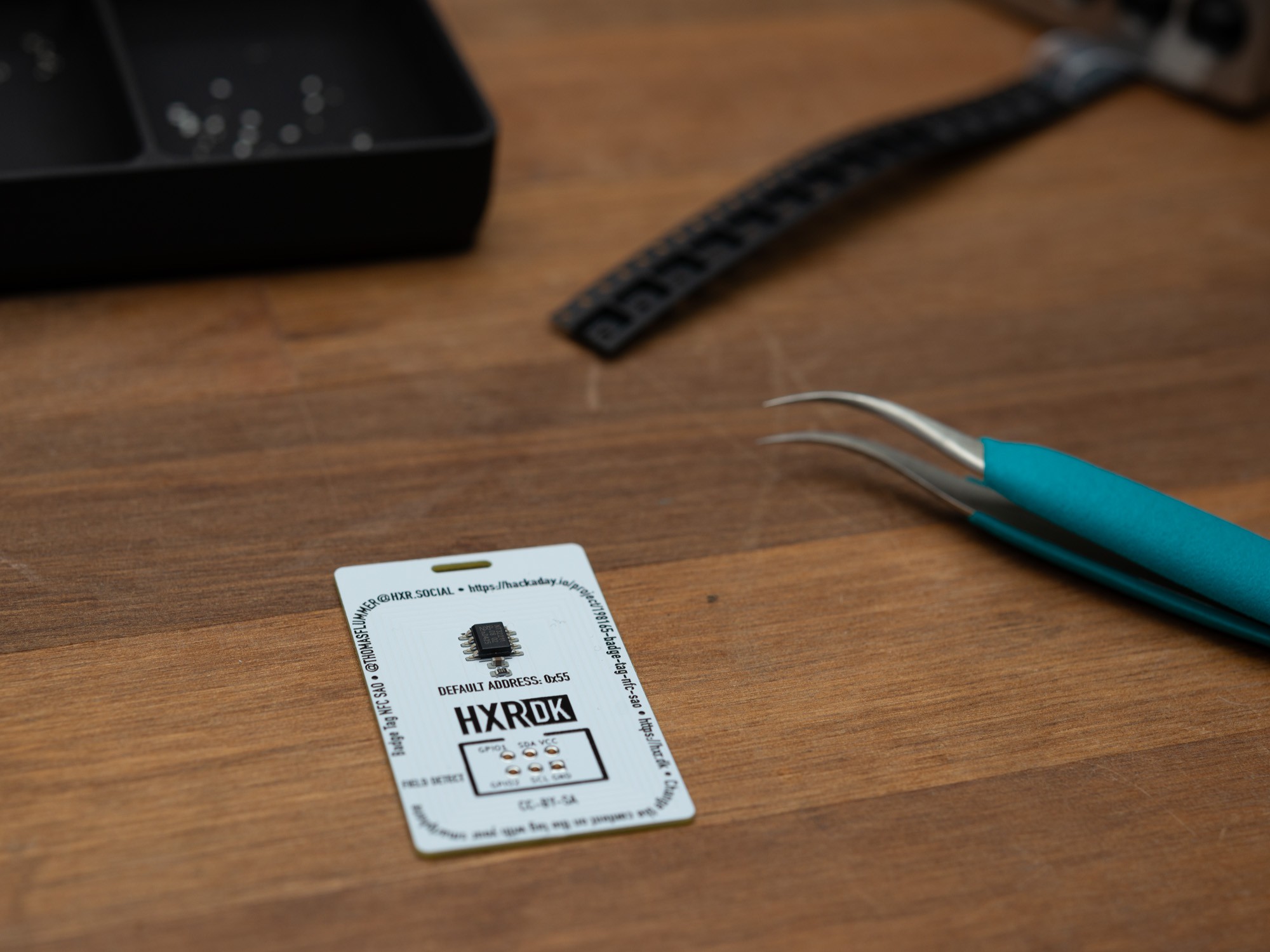
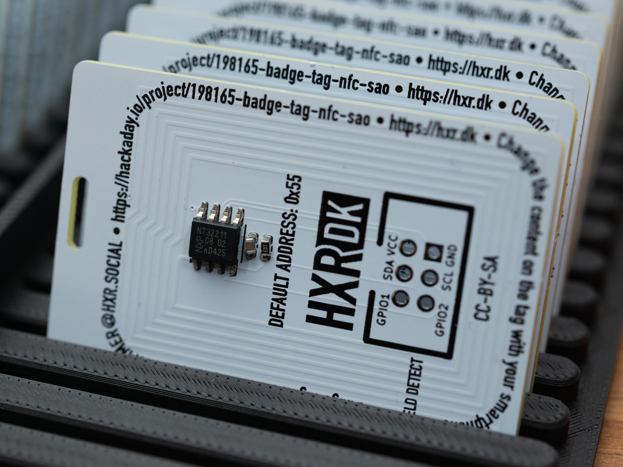
The PCB is only 1mm thick, making it look more than a card, even though it's much smaller than a regular one.
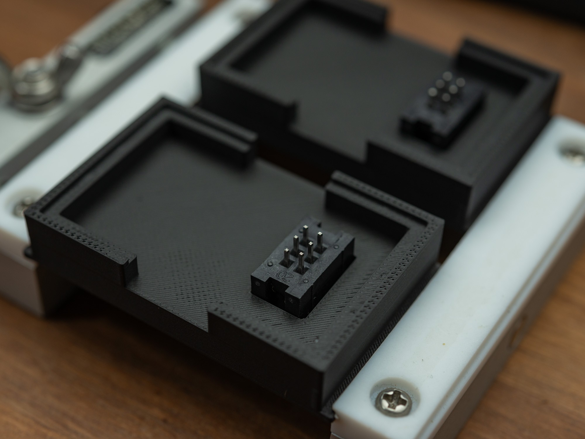
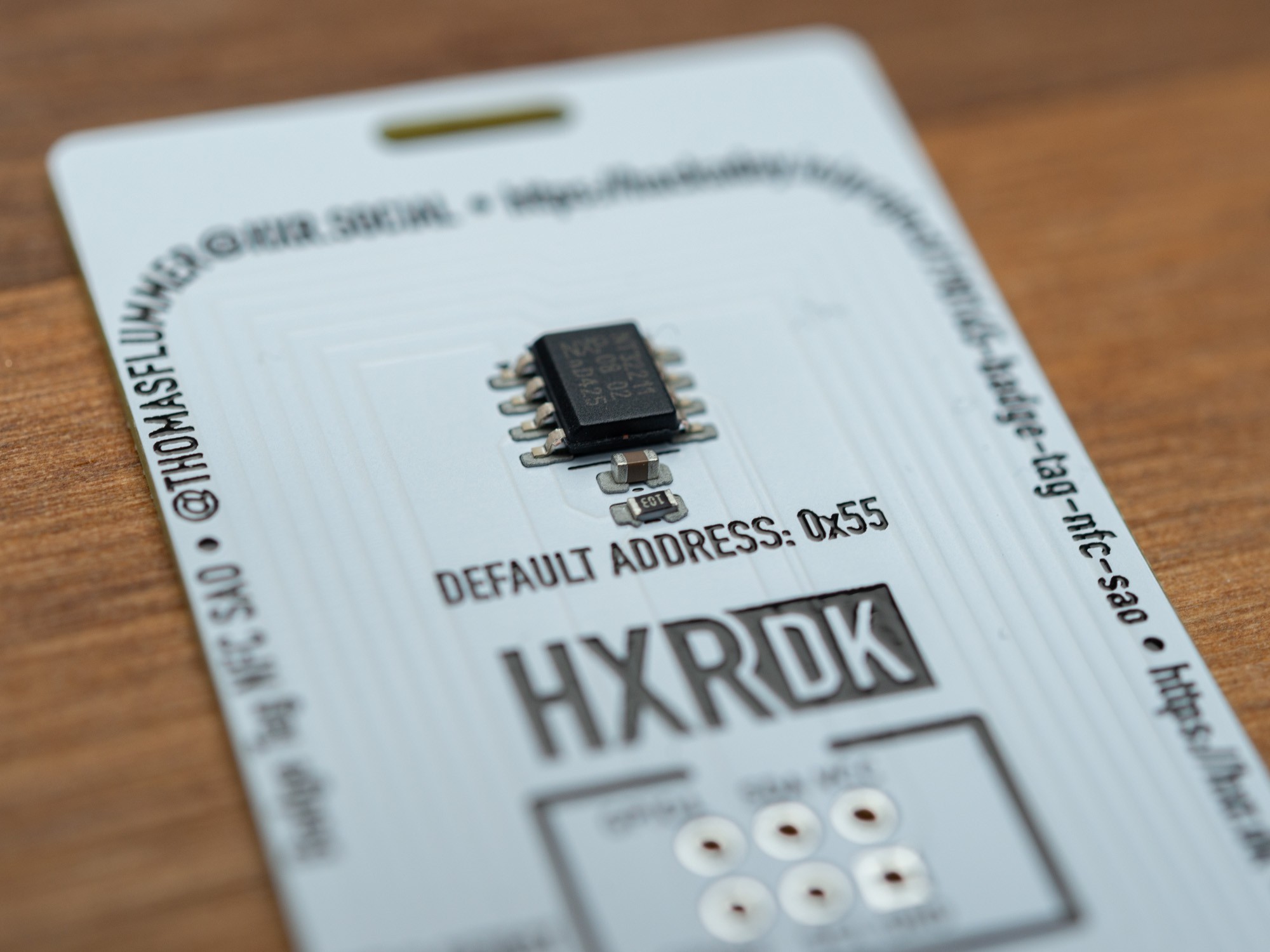
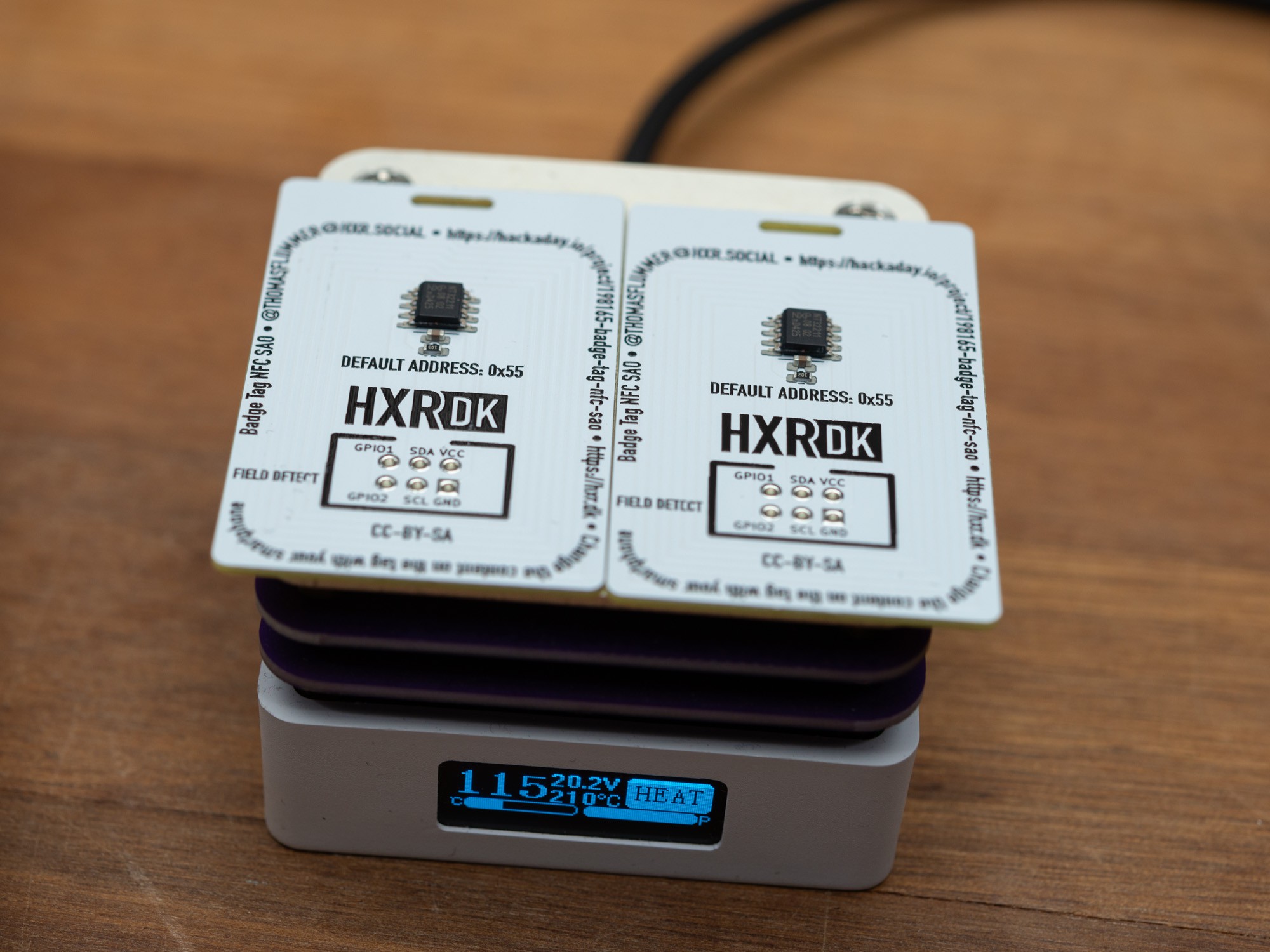
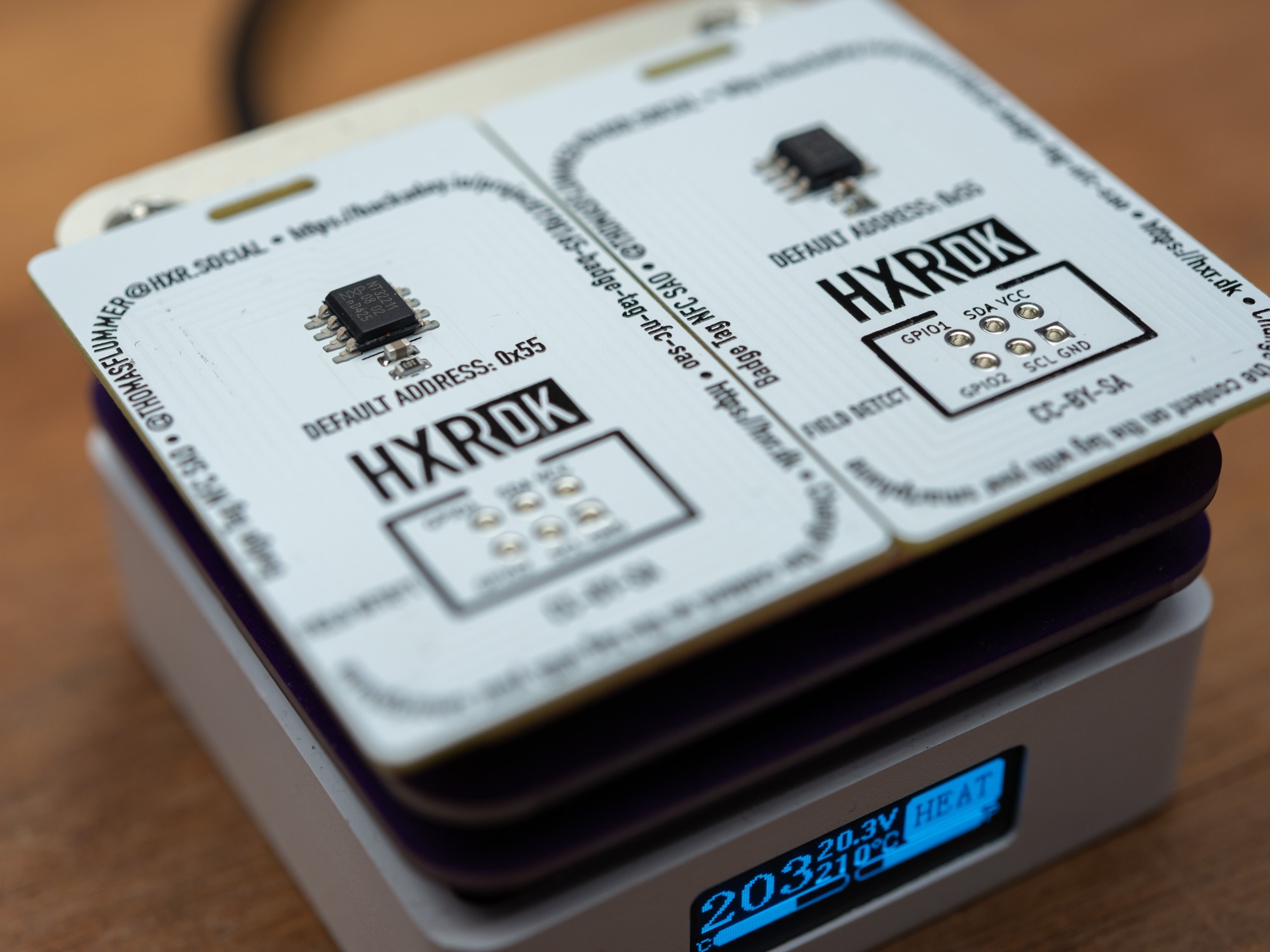
The SAO connector is the through hole variant, to help prevent it from breaking off, but a variant with an SMD connector could also be made, though the elements on the back might need to move a little to not mess with the trace antenna.
Usage
In the top of the SAO is a little cut-out, similar to those used for attaching the badge to a lanyard, but this does double duty, and is also used for an SAO leash, for those that would like to secure their SAO, from accidentally falling off and disappearing.
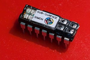
The name field in the bottom can be used to add the wearers name (Ultra Fine Point Sharpie works well) and the icons in the top can be covered, to indicate areas of expertise or interests.
Programming the tag
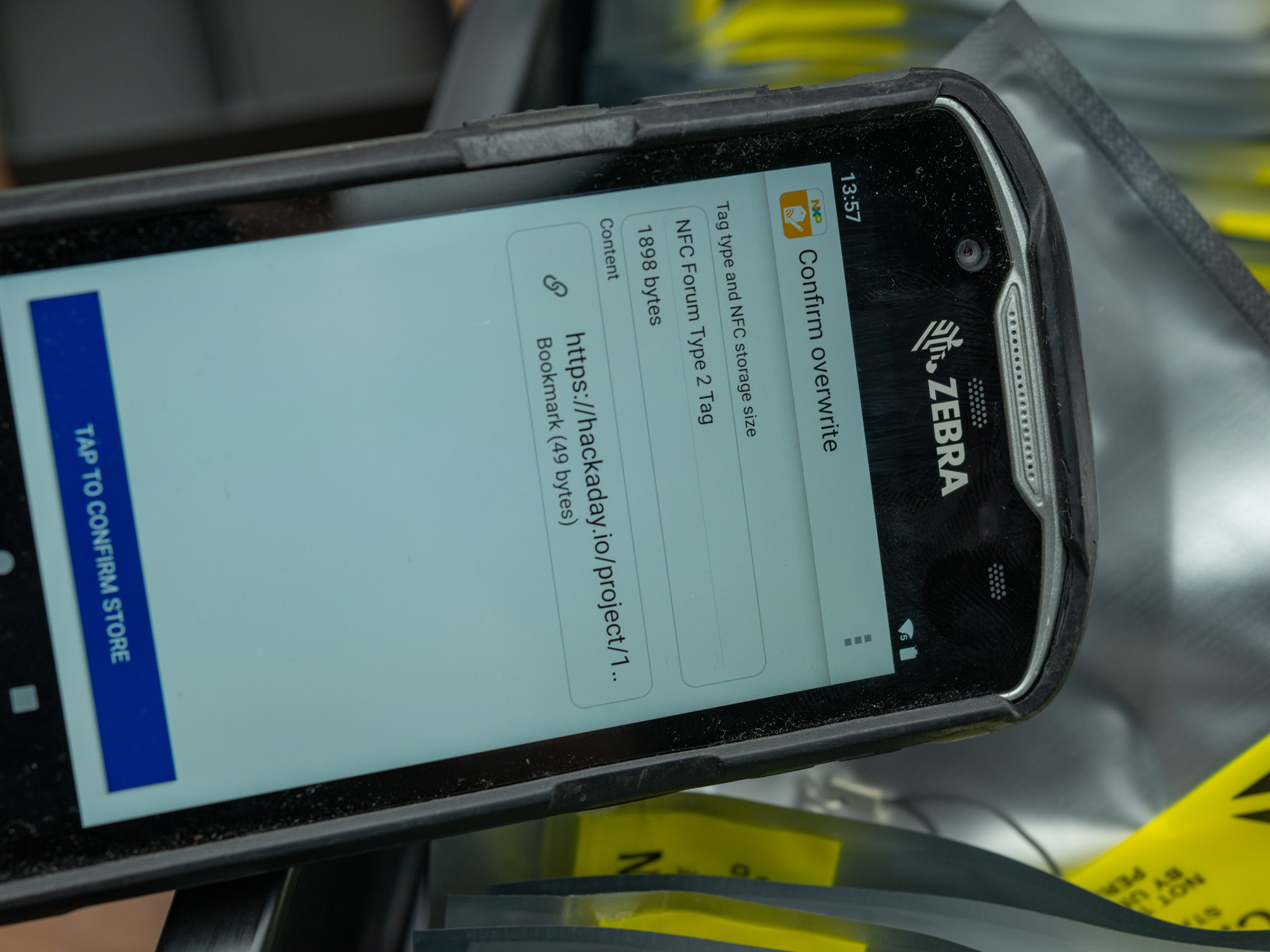
The easiest way to add content to the memory on the tag is using an app on a smartphone equipped with NFC. If the tag isn't NDEF formatted, that is the first thing and that should probably be done on an Android device, and iPhones seems to have some trouble there.
After formatting, one or more records can be added.
NXP TagWriter (available for both Android and iOS) can do this. Another one is NFC Tools.
NFC Tag use
When a reader (eg. in a phone) is powering up the tag, the chip indicates this via the Field Detect signal, that is connected to GPIO2 on the SAO port, letting the badge know that the tag is being accessed.
If you would like to provide other people with contact details, those can either be put directly on the tag memory in an NDEF record, or (eg if you would like to share details with people having an iPhone), you can put a URL in an NDEF record, that points to a vcard file online.
Accessing the memory via I2C
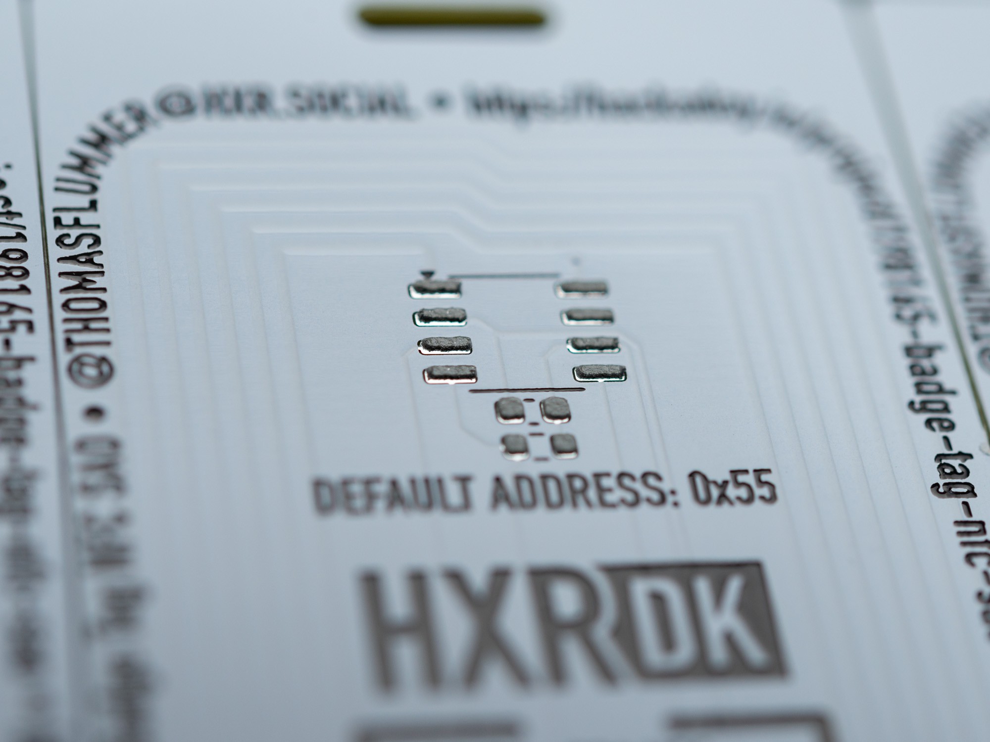
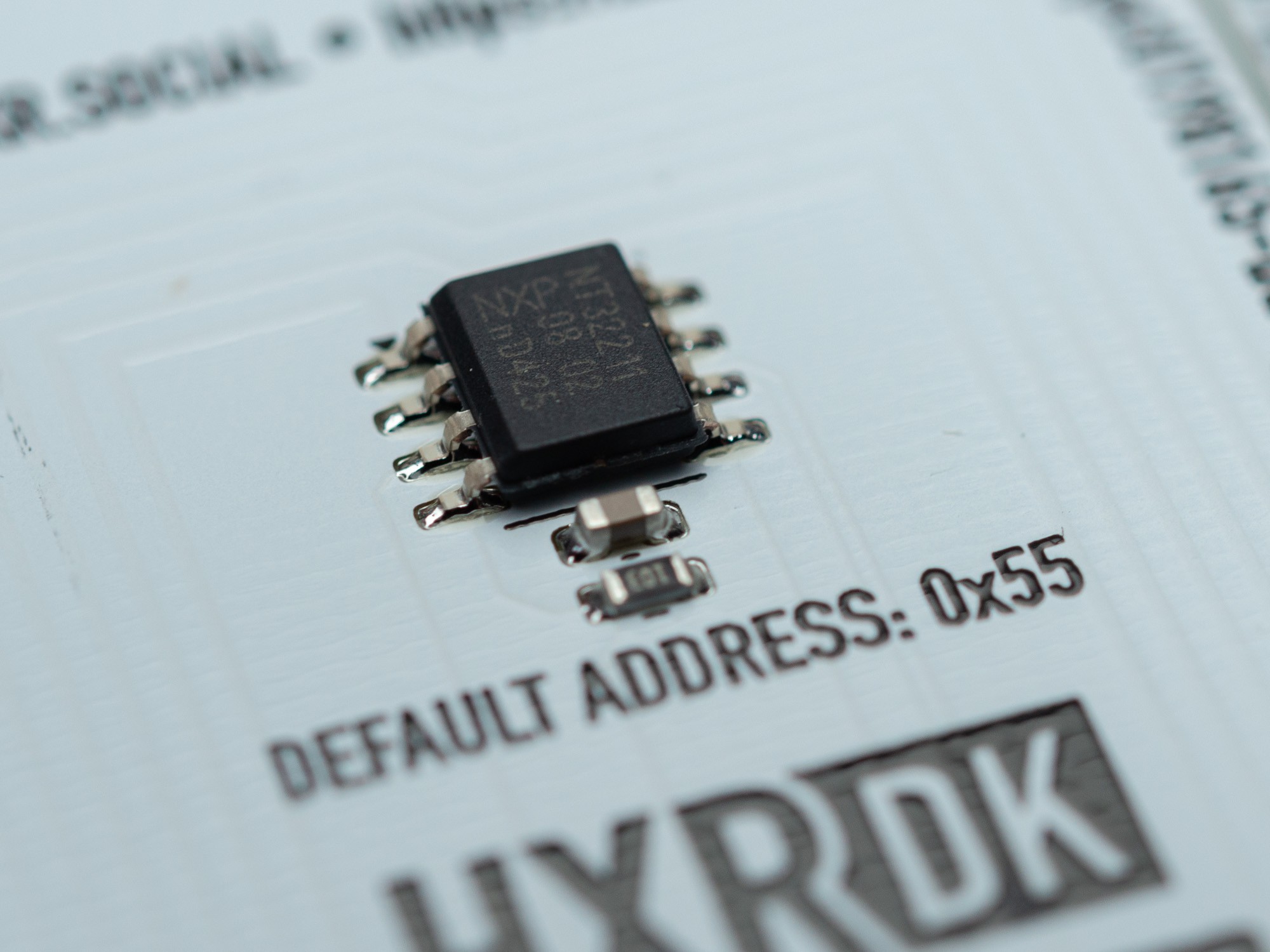
The same memory, that can be programmed using a smartphone, can also be accessed from the badge, via I2C. The default address is 0x55, but that can be changed via the I2C interface, in case there are conflict on the bus.
Be carefull when configuring the memory and the access controls, as it is possible to close off write access from either the RF side (eg. an app on a phone) or the electrical interface (I2C) or BOTH, in which case the tag has turned into a read only device.
 Thomas Flummer

 Reiko
Reiko
 Ralph
Ralph
 leumasyerrp
 alnwlsn