Thomas Flummer
-
Packaging and Programming
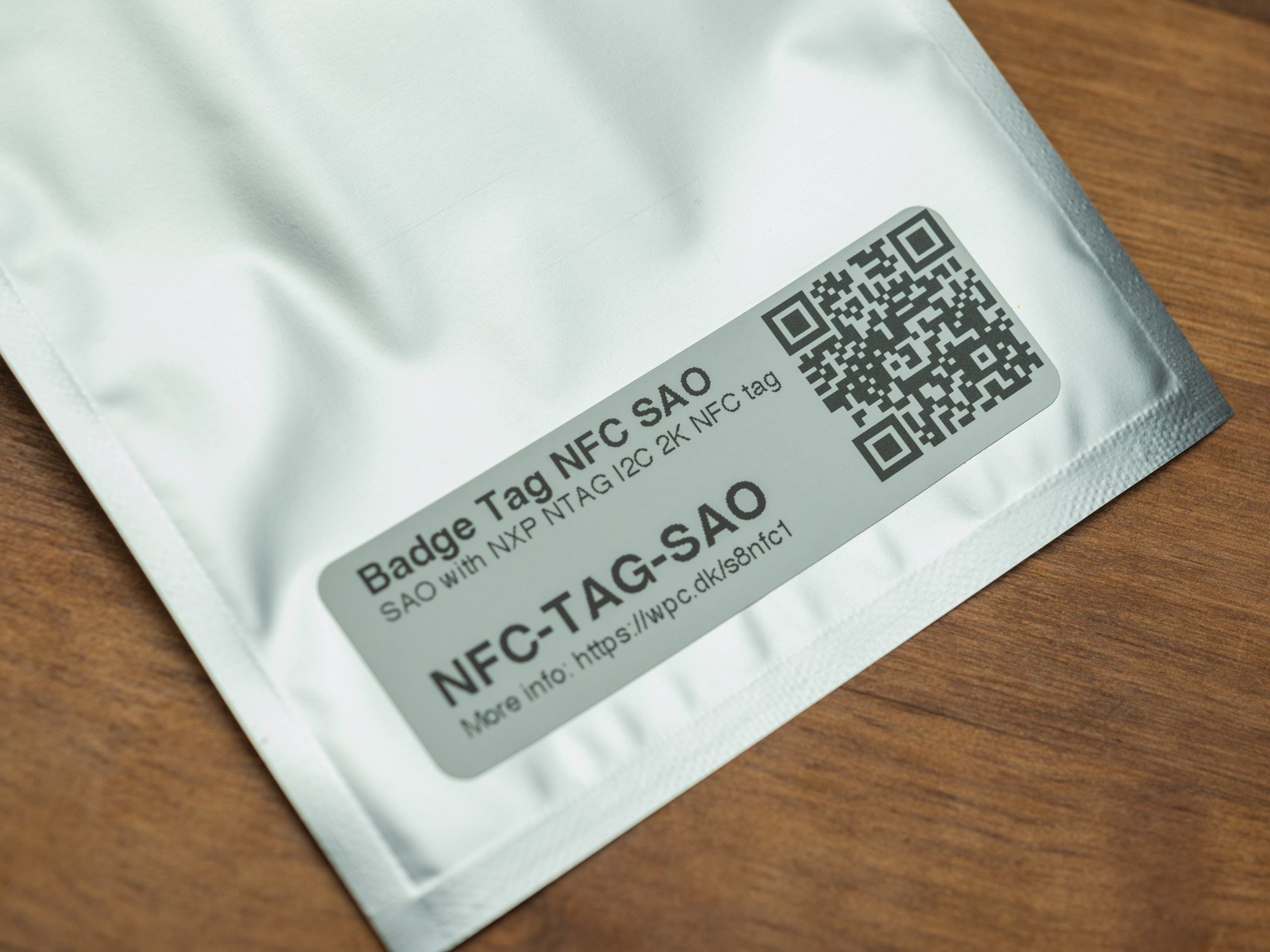
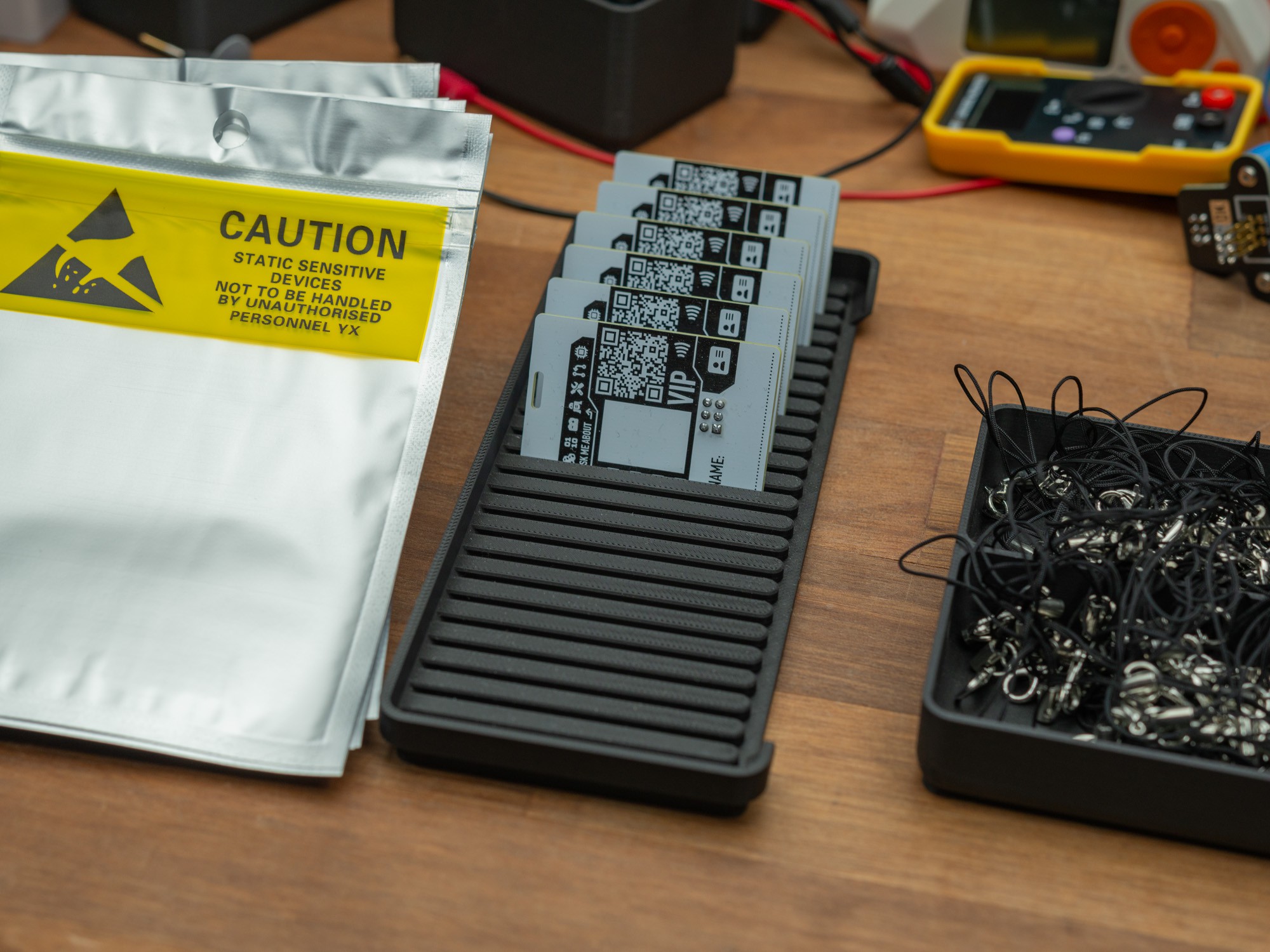
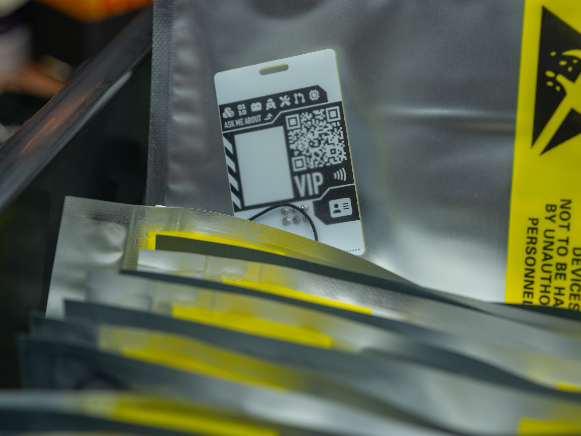
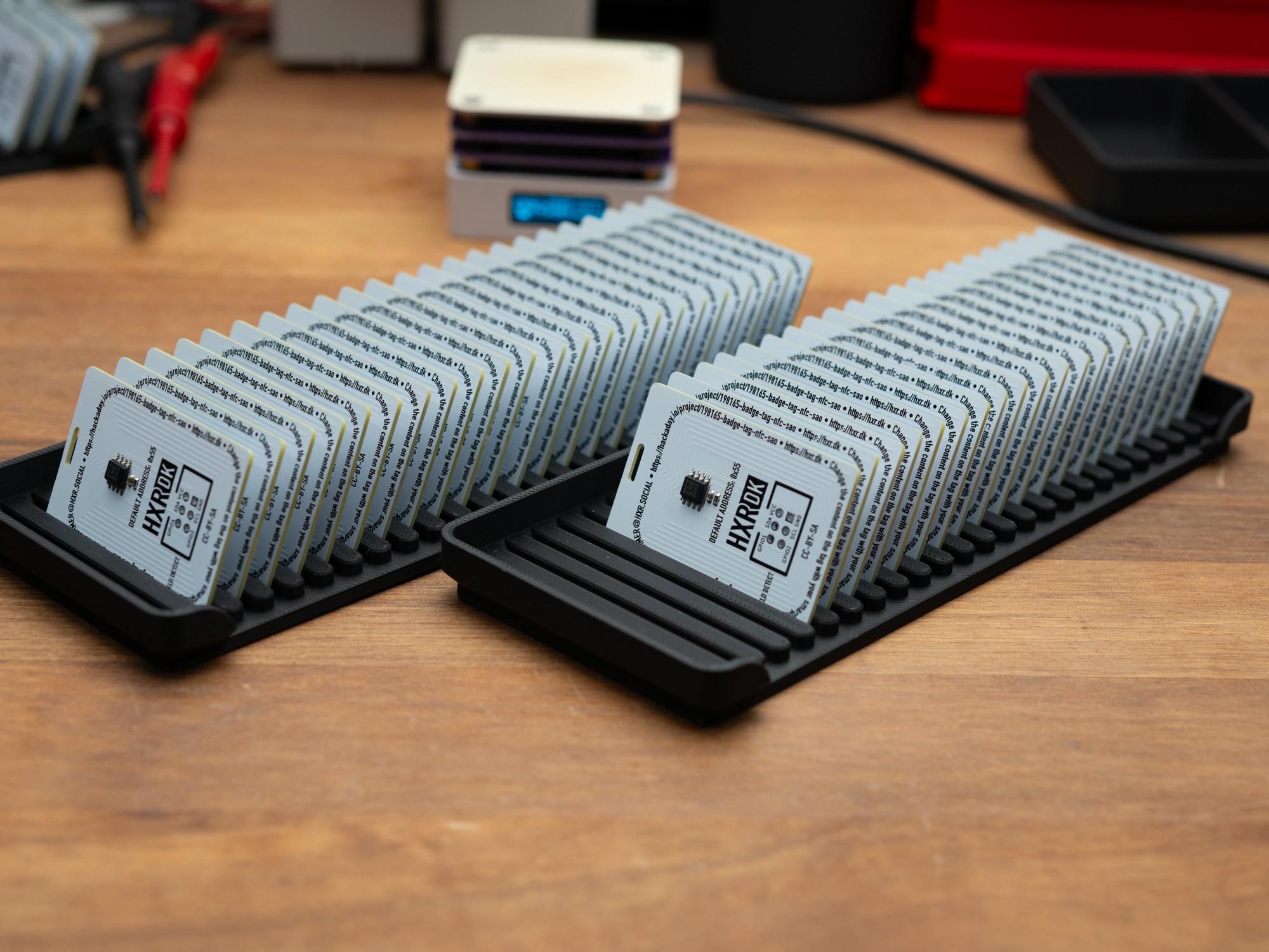
10/27/2024 at 15:47 • 0 commentsI have decided to pack these up in a small ziplock bag, together with the SAO leash (kind of a small lanyard for this tiny badge, and an extra security if it should fall off a badge).
![]()
I have labeled the bags, with information and a QR code linking to this project (via short url).
![]()
One of each in the bag, and then close if up.
![]()
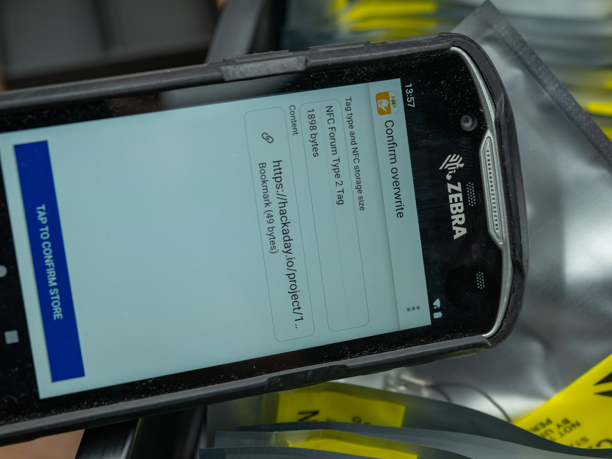
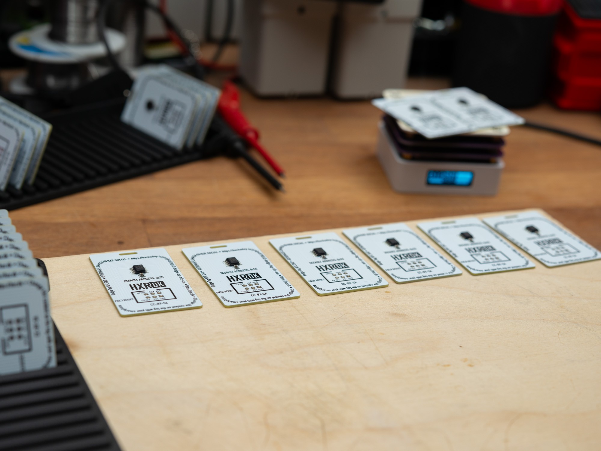
As programming these can be done via the "radio" interface, I simply used an Android device running the TagWrite app to first format and then program the tags to hold a URL.
![]()
Having the tags formatted as NDEF, allows iPhones to also use these. TagWriter is also available for iOS, but it won't do the initial formatting of a blank tag.
-
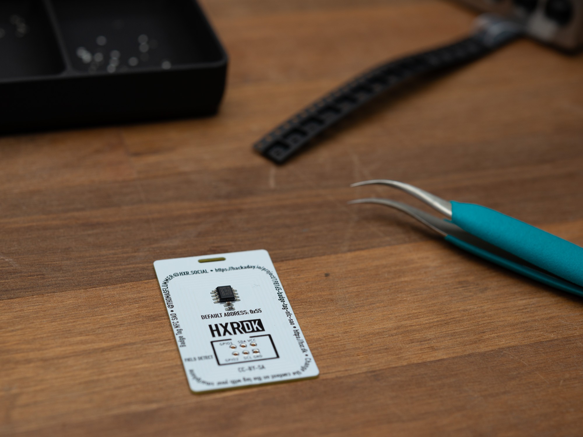
Through hole assembly
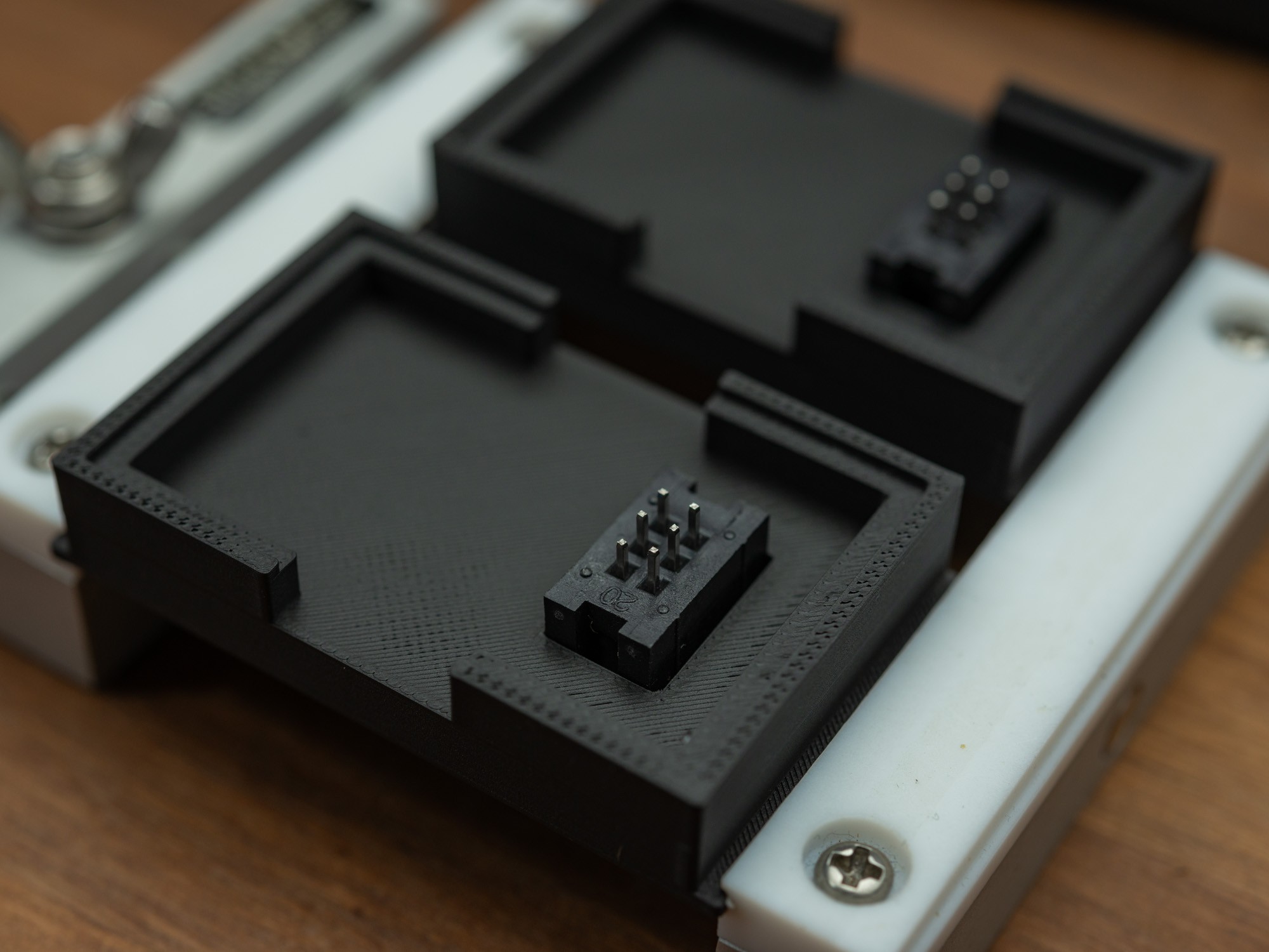
10/27/2024 at 15:39 • 2 commentsFor these, I used a 3D printed jig to hold the connector and the PCB in place. It's designed with a little bit of space, to make it easy to put in the connectors and pul out the finished assembly, but it's tight enough to have the connector sit pretty straight with the board.
![]()
The jig also have a small notch to make sure the connector is oriented correctly, which did save me a couple of times.
![]()
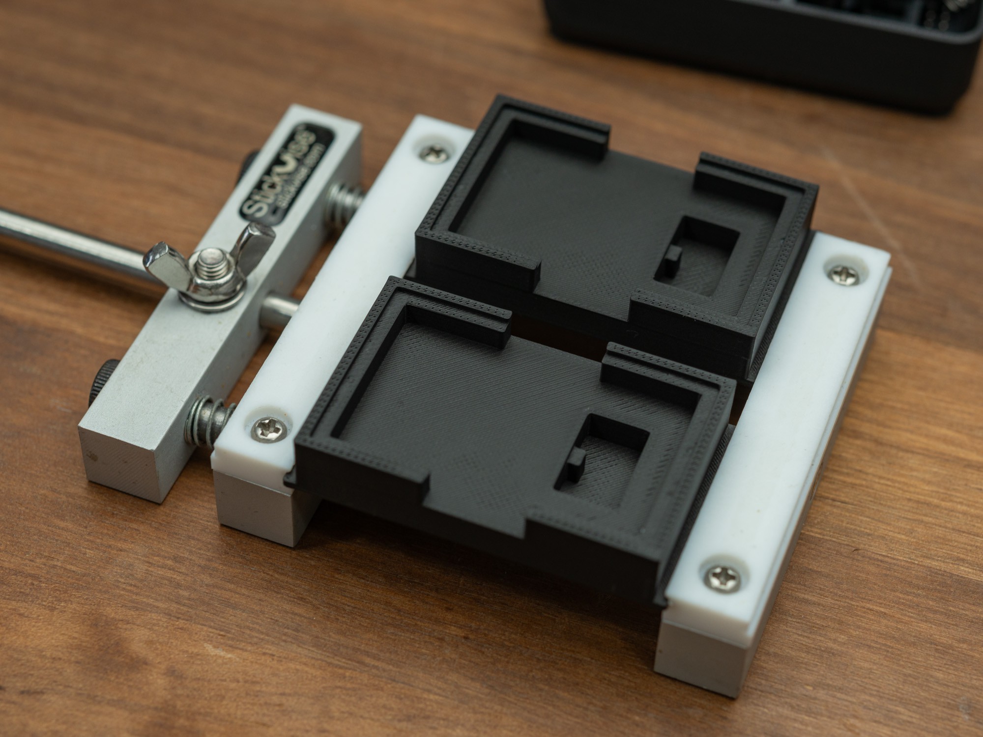
The PCBs then sin on top, and the weight of the Stick Vise, helps it to stay put, when using both hands to do the soldering. I made to jigs in an attempt to optimise context switching, and it worked quite well.
![]()
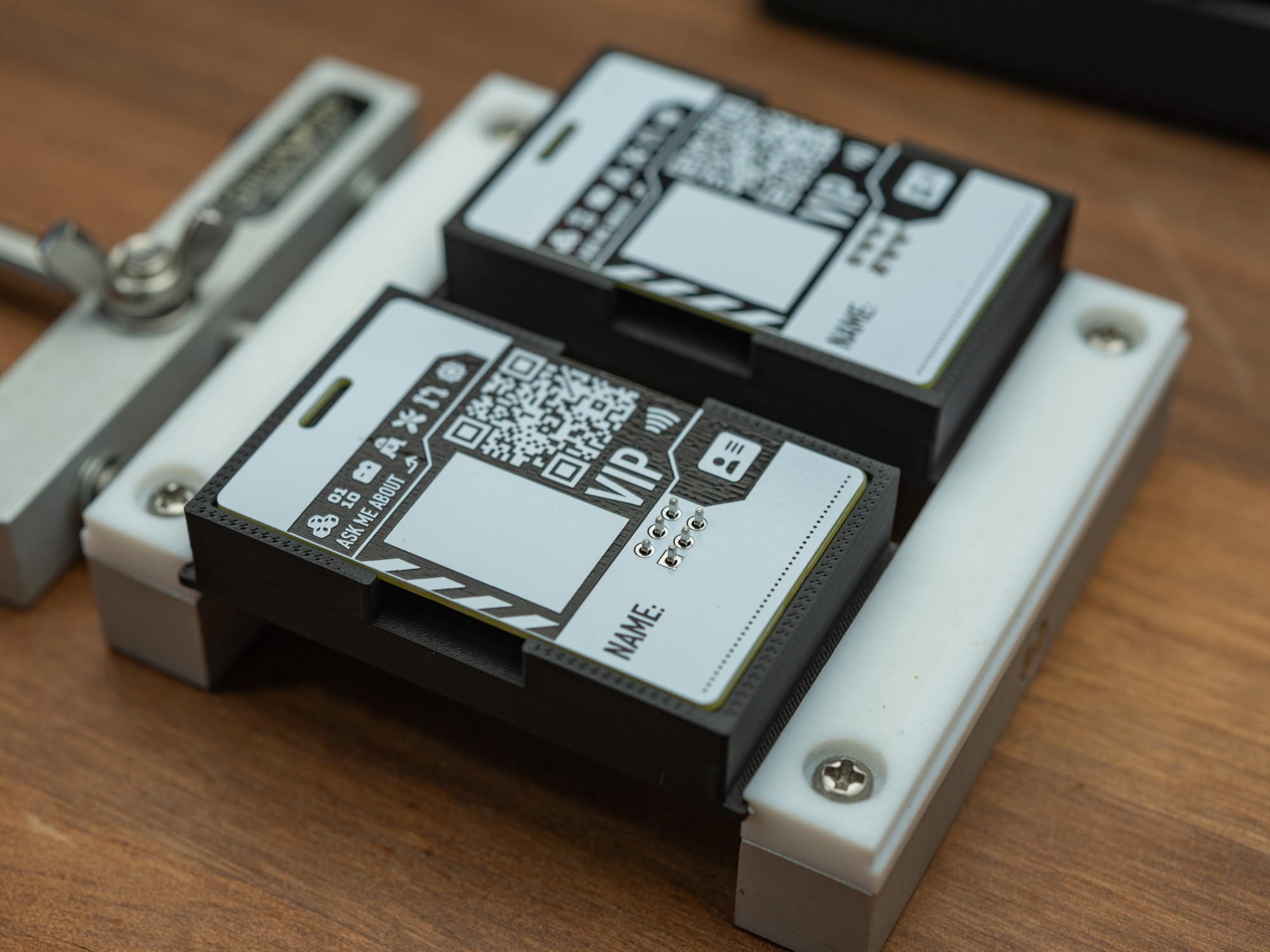
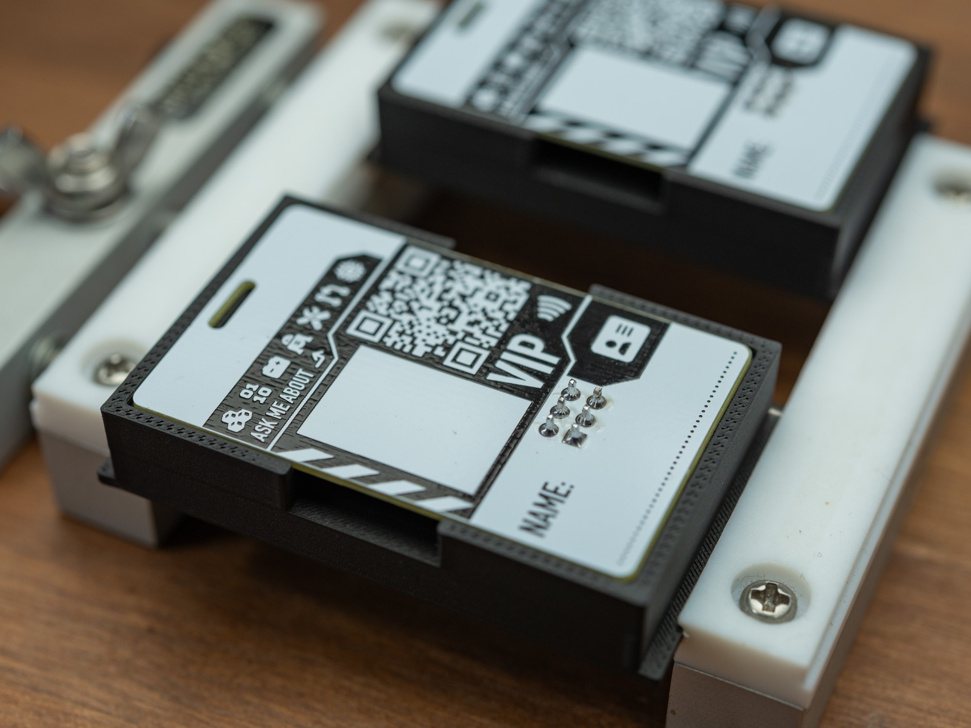
I manage to solder all the boards before it started to get boring.
![]()
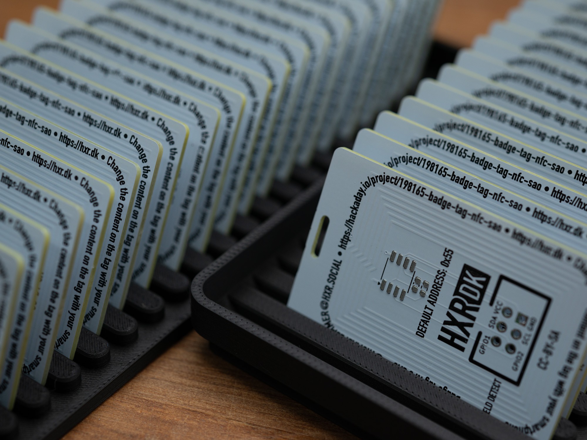
The trays only fit half as many, when the connectors are mounted, but they do stack.
-
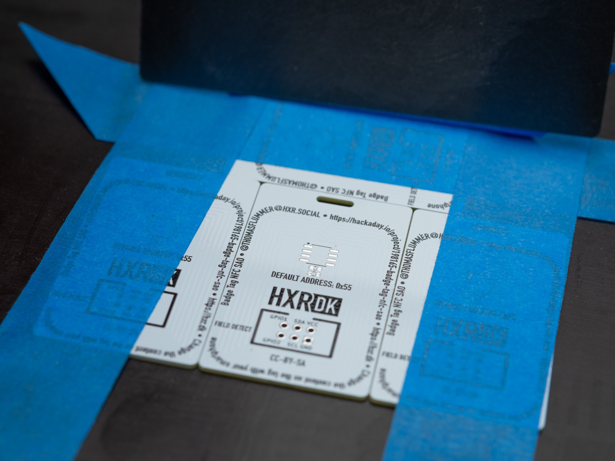
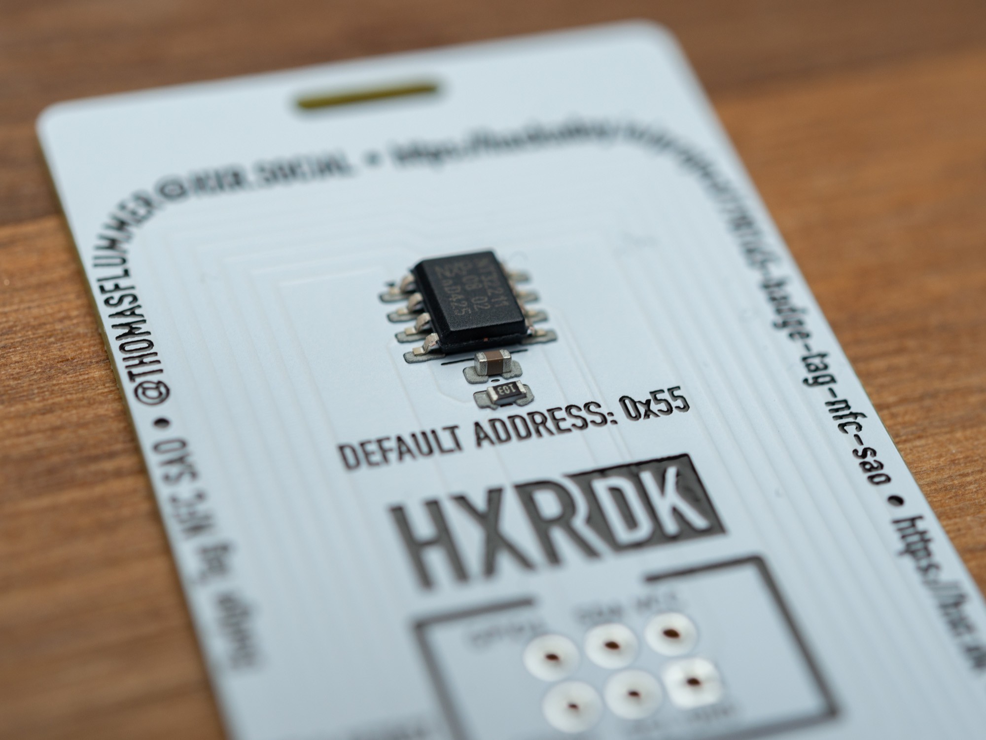
SMD Hand Assembly
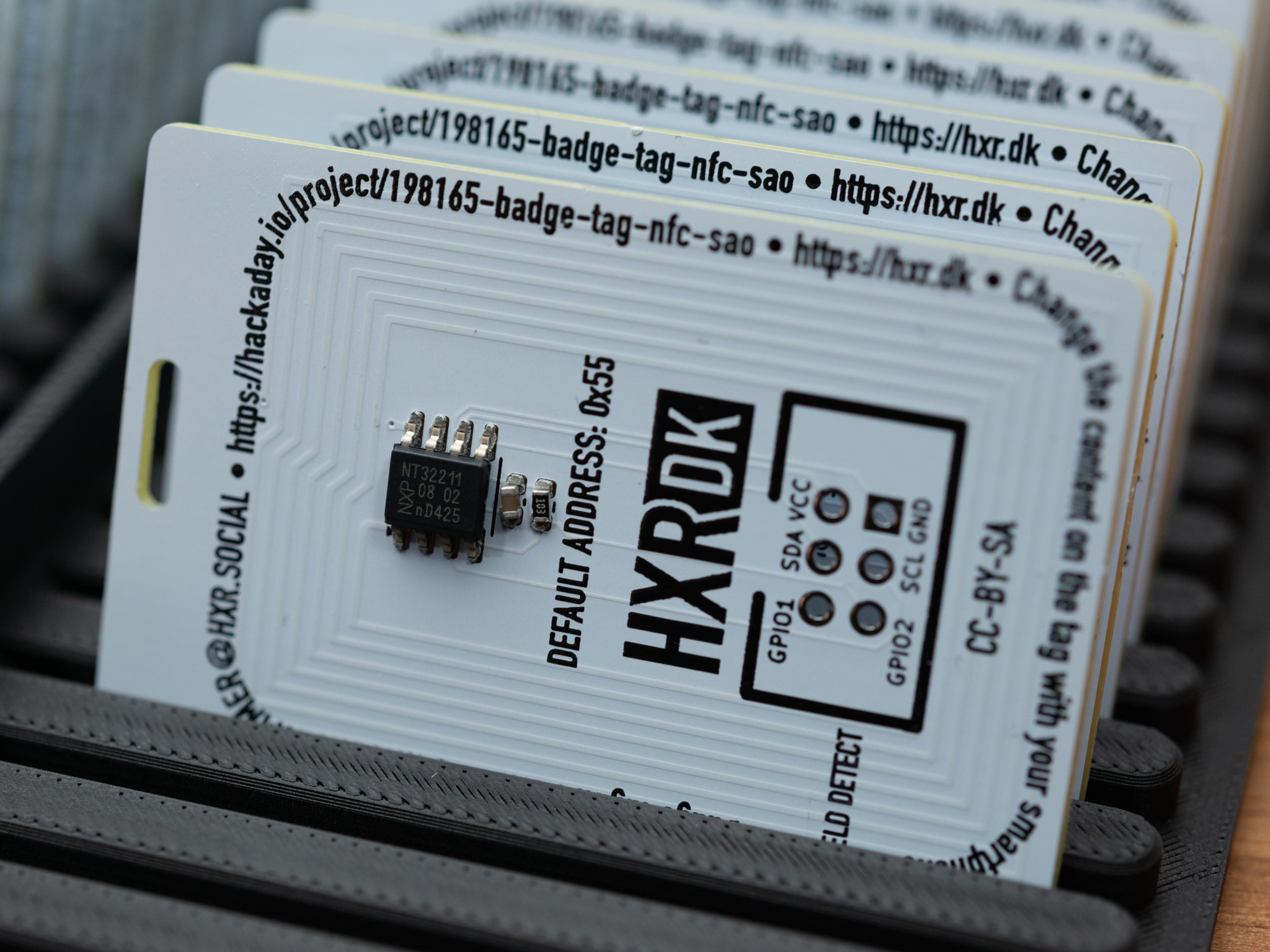
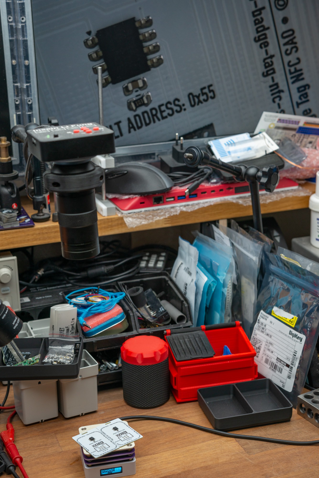
10/27/2024 at 15:30 • 0 commentsFor this project, I decided to hand assemble them, since there was only 3 SMD parts, and I choose the rather large variants. I have tried the tiny variant of the NFC chip, and it's not worth it for this project. Even PCBA houses get that one wrong and last time I used that, I had to manually rework almost all PCBs to get them working.
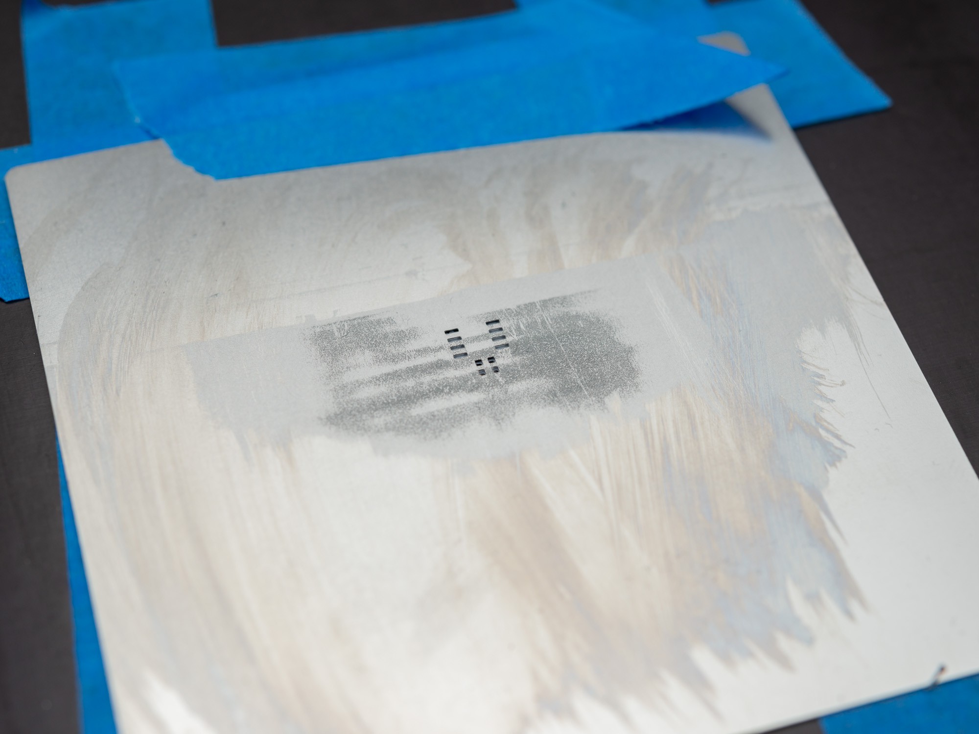
I use a simple setup with other PCBs taped to a piece of plywood for the stenciling setup.
![]()
The stencil is then aligned and hold in place with a "hinge" also made out of tape.
![]()
If you are thorough in aligning the stencil and carefull not to move it, it works quite well and no problem for this size of components
![]()
This is my setup, with a stack of new PCBs, and the PCBs that have had paste applied in the tray to the left.
![]()
I have a camera based microscope that I use to check the paste application.
![]()
After applying paste to all the boards I moved on to component placing. I'm using the 3D printed trays to store the PCBs in between the different steps, and it's very convenient to be able to move a full tray.
![]()
Generally, when doing hand assembly, i place a given part on all the PCBs, and them move on to the next, mainly to that parts are not mixed up, but for this design, each part is clearly identifiable and I decided to simply pour out a bunch of each and do it one board at a time.
![]()
I use curved tweezers and this is a pretty good quality, making it fairly easy to gram onto small jelly bean parts like the resistor and capacitor. These are just 0603 parts, so not THAT small.
![]()
I give the parts a small "tap" to make them sit in the paste and they sit well enough to put the PCBs back in the trays sitting on the side.
![]()
The small components doesn't need to sit absolutely perfect, as the surface tension of the solder will pull them into place.
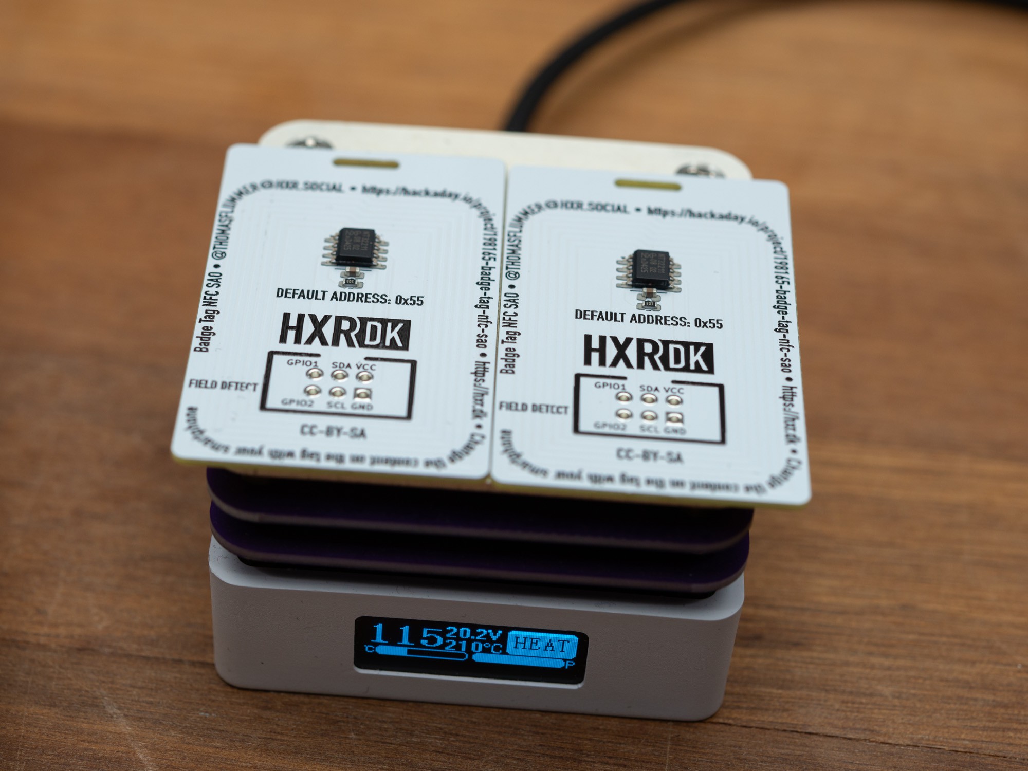
I use a small hotplate for soldering, and it just fit two at a time.
![]()
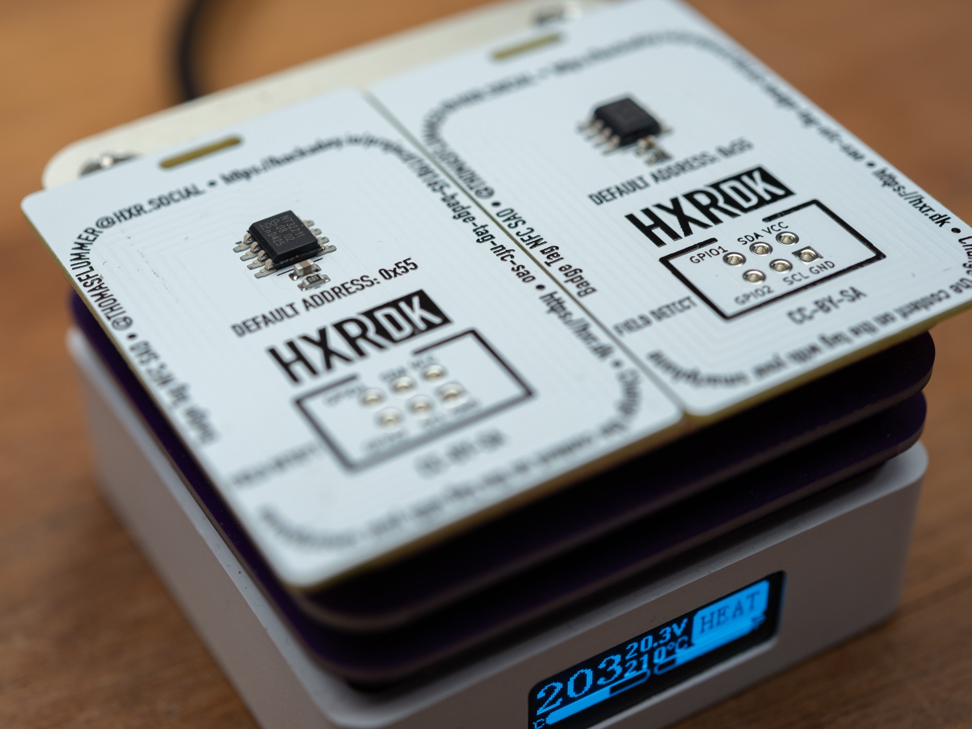
This is the first ones heating up, but for the following sets, I did not cool down the hotplate in between, to save time. It's probably not ideal to chock the PCB and parts putting them directly on a hot plate, but it seems to work OK and the PCBs did not discolor (I keep the temperature at about 210°C)
![]()
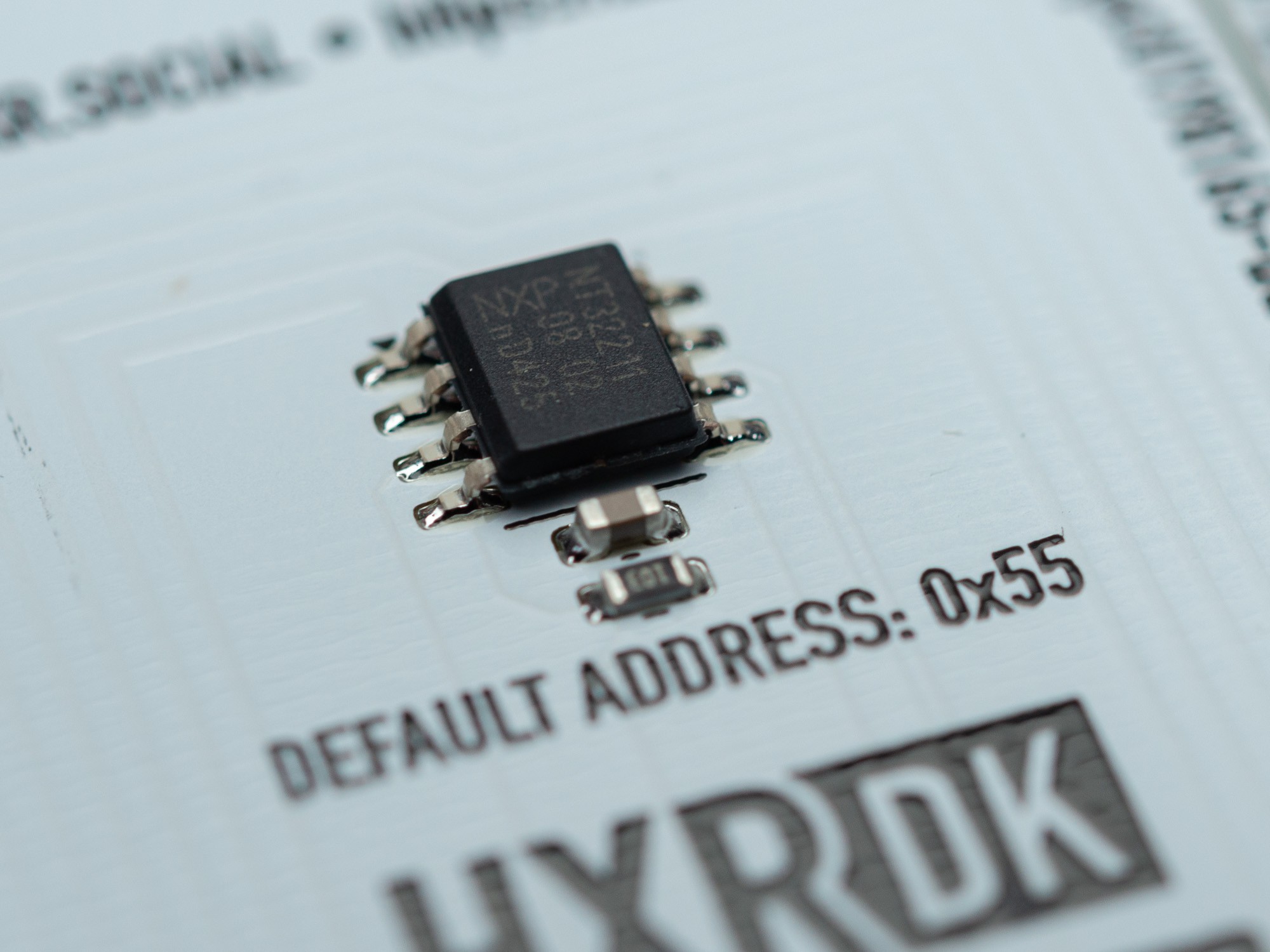
The solder for the small parts melt first, then for the larger chip.
![]()
I use the microscope for monitoring the reflow process
![]()
And let the warm PCBs cool a little on a piece of scrap wood
![]()
Before putting them back in the trays, ready for further assembly.
![]()
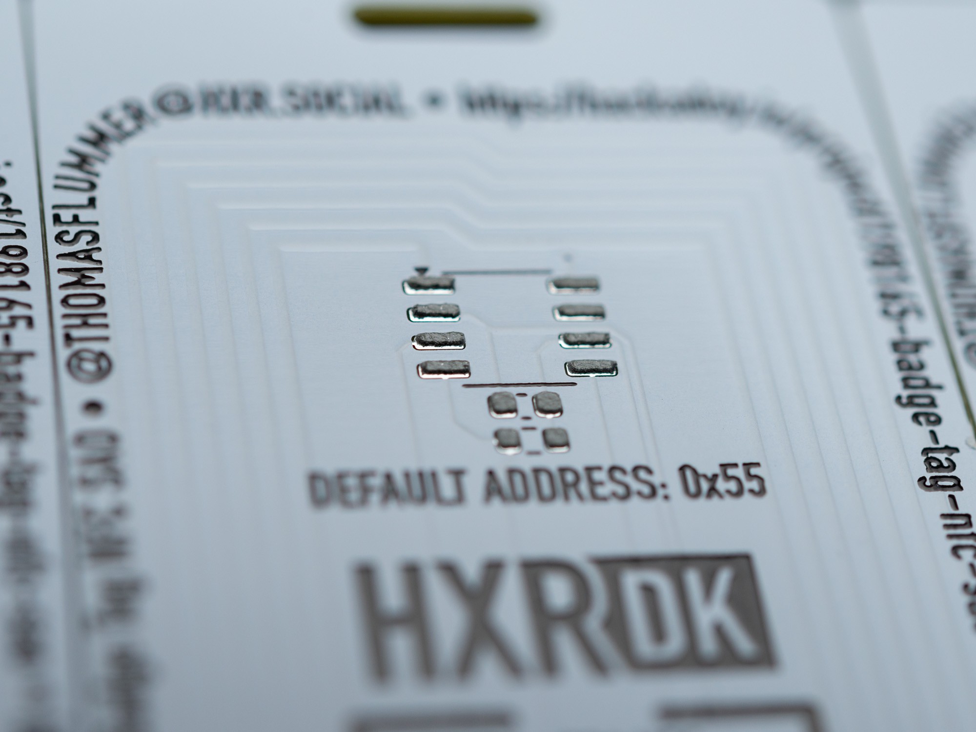
Badge Tag NFC SAO
Adding some of the traditional badge stuff to any badge