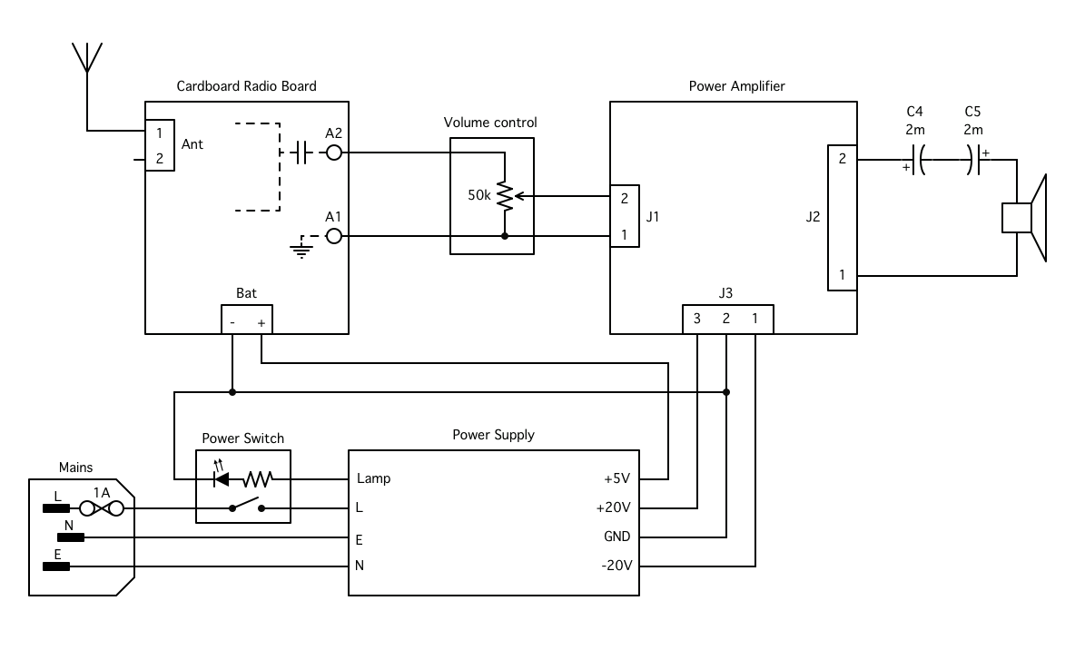
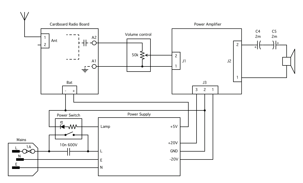
Block Diagram
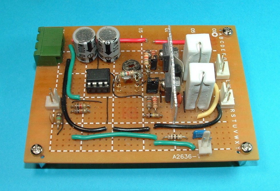
Power Amplifier
The power amplifier design is based on ideas from these pages:
https://sound-au.com/project3a.htm
https://sound-au.com/amp_design.htm
My design is essentially the one from the first link above with the input stage replaced by an op amp.
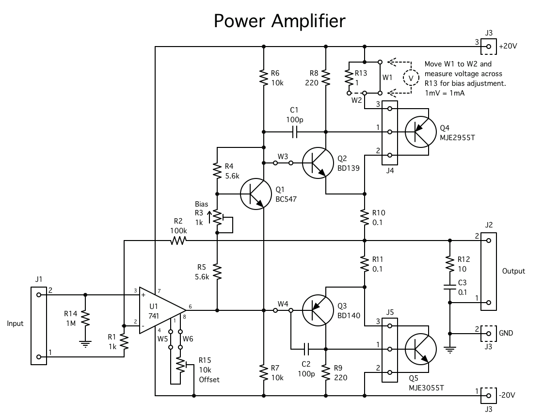
The use of Sziklai pairs instead of Darlingtons improves temperature stability, since the bias conditions depend mainly on the temperature of the driver transistors (Q2 and Q3) which get much less hotter than the output transistors.
C1, C2, R12 and C3 are included for stability.
The ground reference for the input is taken from the earthy end of the volume control. I found this to be necessary to prevent hum entering via differences in ground potential between the RF board and the amplifier board.
R14 is present to keep the DC conditions stable if the amplifier is powered with the input disconnected. In this state, the circuit becomes a voltage follower with its input grounded.
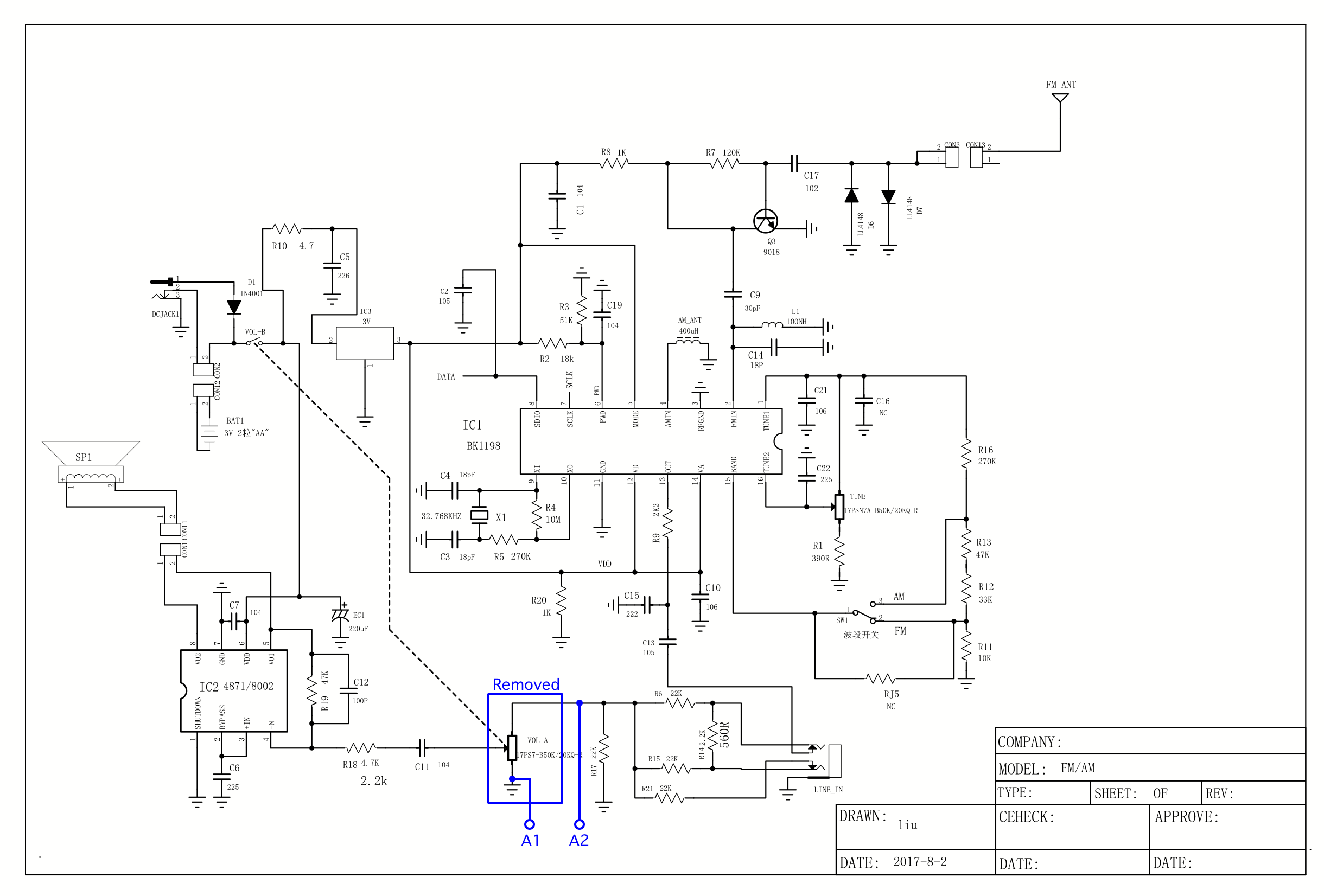
Modifications to Cardboard Radio Board
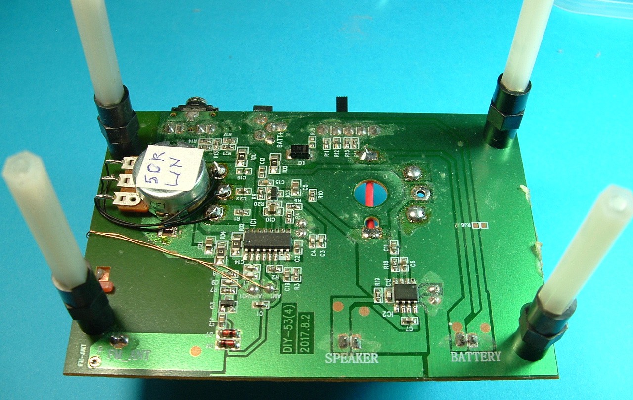
The Cardboard Radio RF board comes pre-assembled and has two potentiometers mounted on it, the volume control and the tuning control. I removed the volume control so that I could mount it on the front panel. I decided to leave the tuning control on this board for now and make it accessible from the back, because I don't want to make it too easy for my mother to accidentally disturb the tuning. I ended up remounting it the other way around, though, because it turned out to be more convenient to have the shaft pointing out of the other side. I may make some changes to the tuning system in the future.
I took the audio output from the pad where the top end of the volume control was connected. The exising audio amplifier on the board is not used.
The red wire is bridging a ground connection that was previously completed by the removed volume control.
Power Supply
There's nothing very remarkable about the power supply. It provides +/- 20V for the power amplifier and +5V for the RF board.
The reason the 5V regulator is fed from a separate rectifier is that I was getting a pop from the loudspeaker a second or two after powering off with the volume turned down, and I found it could be prevented by ensuring that the power amplifier remained powered while the RF board was shutting down. Giving the 5V its own feed from the transformer allowed me to ensure that it ramped down first during power-off.
The capacitor across the power switch is another measure to prevent noises when powering on or off.
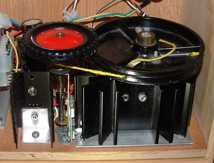
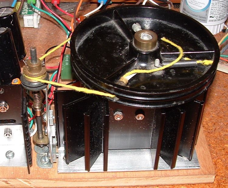 The spring presses the small pulley against a rubber grommet to provide a bit of friction.
 ric866
 Jared Young
 Paul
Paul
 Toney
Toney
Just wondering if you have the schematic in some ECAD format like KiCad, Eagle or ... Thinking it might be a design for tinkering with ngspice simulation in KiCad.