It seemed to take OSH Park forever to fab these PCBs. I eventually received 3 perfect purple PCBs last Monday (2024-11-04). I populated one of them and immediately discovered a problem. M3 was wired upside down! The source and drain were reversed, so it was essentially a diode connected to the positive supply. When I powered it up the circuit hit the current limit of the power supply at about 2V.
After grokking the problem I set about to re-wire M3. It is almost impossible to skywire a power FET. The gate lead is so tiny and the 3 source pins don't lend themselves to easy connections. I did eventually connect a new AO7405 using 1mm wires. The circuit functioned for a while until the PFET smoked. A dangling 3.3mm x 3.3mm package probably has a 300C/W thermal resistance. Even 1W of dissipation would put it over the 170C limit of the silicon.
Then I remembered that I had some unpopulated small PCBs that used the same footprint as the PFET. It was relatively easy to solder a new AO7405 to the bare board and connect it to the the burner PCB with a few 26 AWG wires. Here's the result:
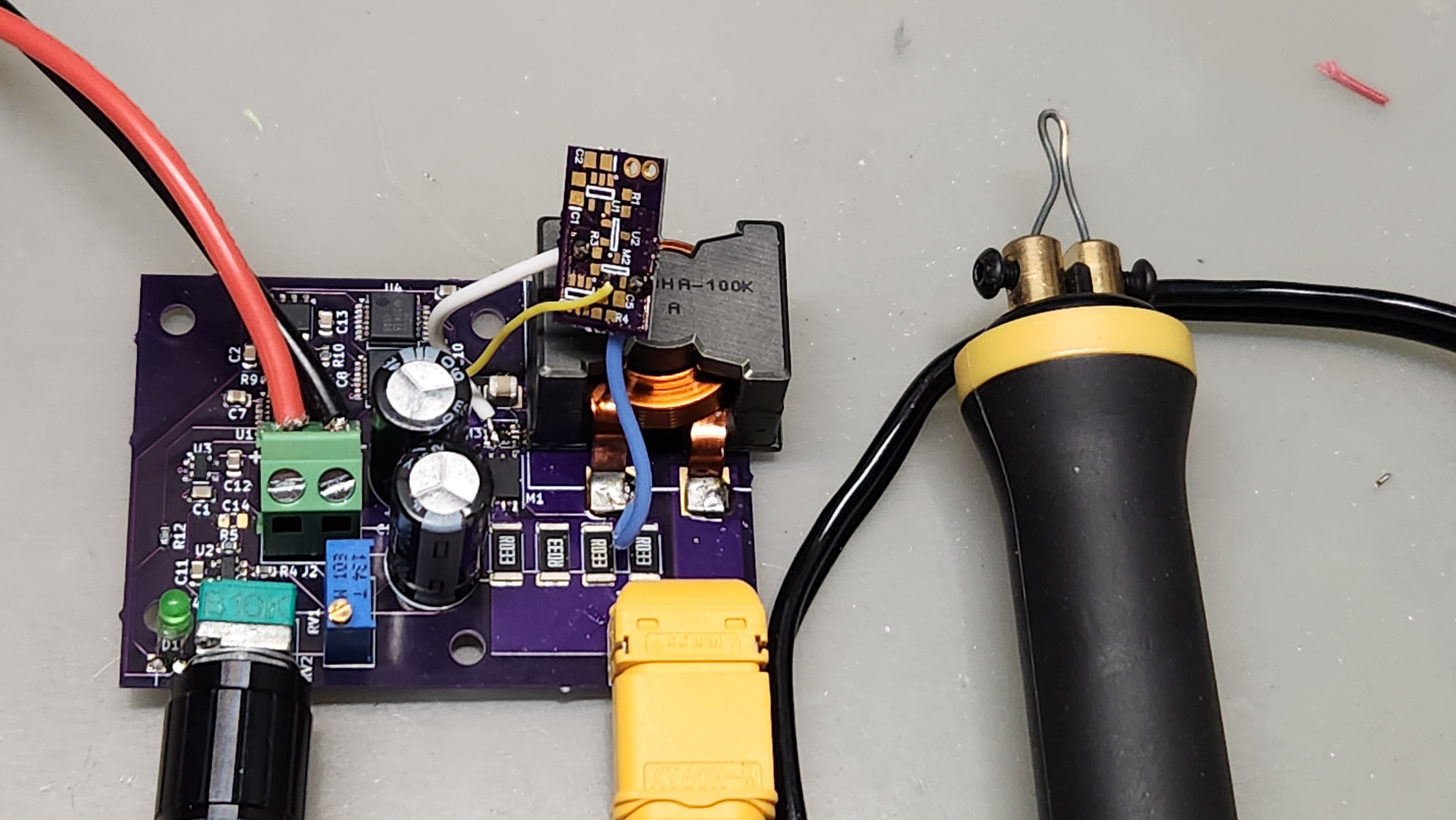
The circuit worked as expected after this fix. I was able to pull about 4.6A from 5VDC and get a satisfying red glow from the tip of the burner. I calculate that the circuit was generating between 12-14A across the heating element.
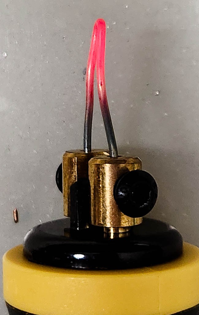
At this point I decided to check the temperatures of the top PFET and bottom NFET to see if there was a problem. The bottom NFET settled out at 47C with 4A (20W) pulled from the power supply. No problem there. The top PFET was pretty hot at 97C at 20W, and maxed out at 117C with 23.5W pulled from the supply. That PFET has a RDSon ~ 10mR, which should not be a problem at these currents (15A). It is difficult to determine if the problem is that the PFET is mounted on a smallish PCB dangling in thin air, or a result of some other unforeseen issue. I decided to err on the safe side and change the design -- using a bigger PFET, both in RDSon (6mR) and package size, 5x6mm vs. 3.3x3.3mm.
So I dug a bit deeper. I got the oscilloscope out of storage and put a probe across the hand piece terminals to get this:
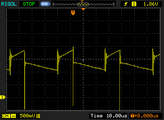
This was taken with the 5V supply reading 2A current draw. Something is very wrong with this. The 0.5V step up and down should not be there. I thought it might be an improper ground reference of the scope, but it did not change with several other ground points. I even dug out my differential probe, which did not record any difference.
I decided to check what the opamp was seeing and got this trace at the opamp output:
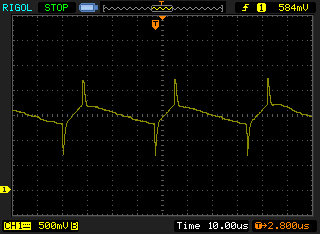
This is more like it, except for the spikes at the transition points. It took me a long time to figure out what is going on: mutual inductance. The handpiece has two approximately 1m long wires running to the tip and back. Those wires are separated by about 5mm. A quick trip to the mutual inductance calculator on the web produced an inductance of around 1.4uH per lead, with a mutual inductance about half of that. When I added the lead inductance and mutual inductance to my SPICE simulation it produced nearly identical results to what I was seeing on the bench.
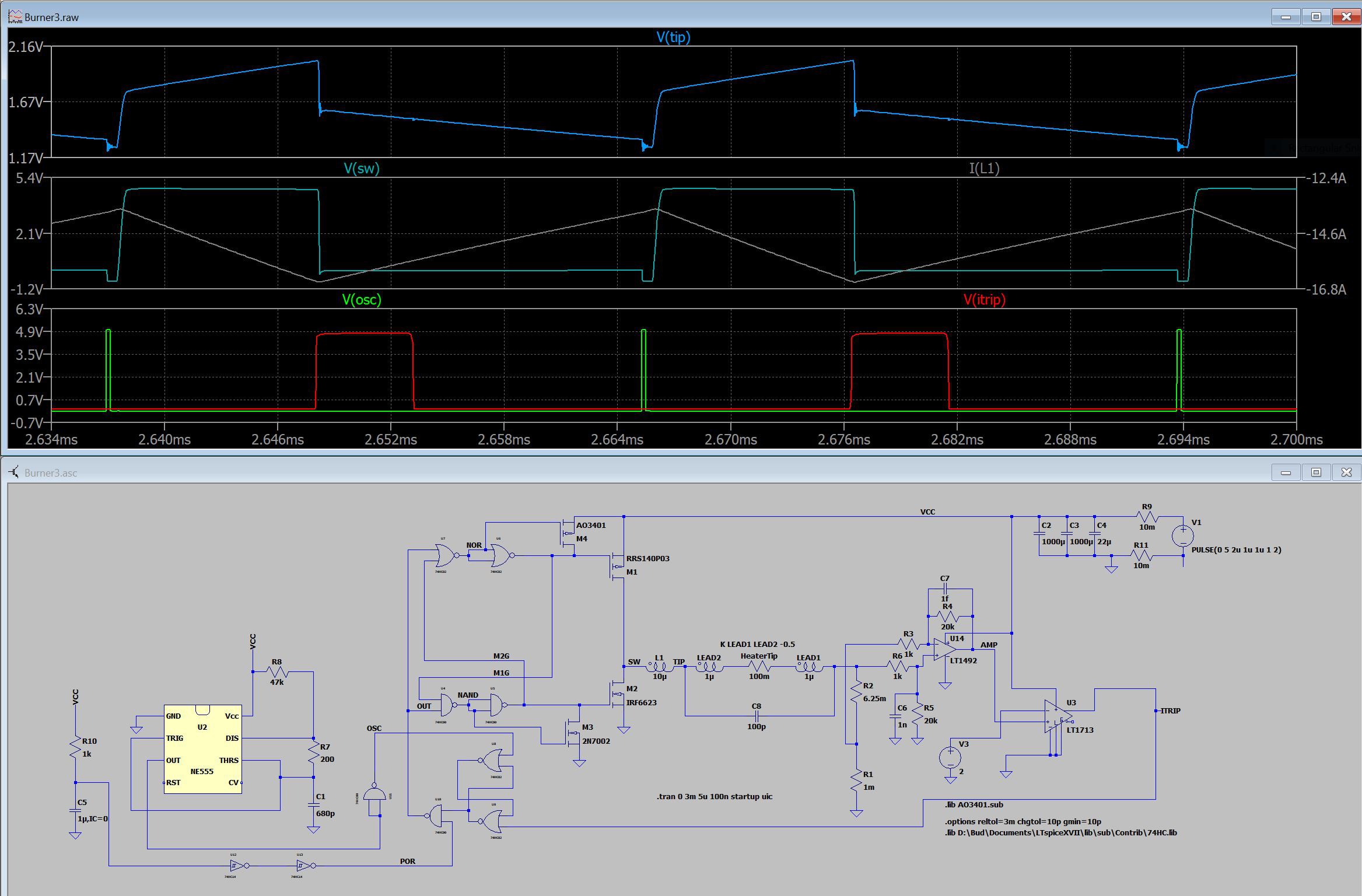
I modeled the handpiece and tip as a 100mR resistor with two mutually coupled inductors, and for good measure a bit of parallel capacitance. The most interesting thing to note is that the current through the handpiece is not affected, and neither is the current through L1. So the opamp output should be a nice triangle, but the glitches don't matter much in the scheme of things as long as the opamp recovers. Adding a 5pF capacitor across the feedback resistor might fix it.
Second Pass Changes
I found a replacement for the PFET -- a DMPH1006UPS. It has an RDSon=6mR with VAGS = 4.5V, comes in a 5x6mm power pak type of package. The downside is that the VDSmax is 12V, so I probably won't be able to use it for many other project. But the advantage there is that the total gate charge, Qg, is quite low at only 72nC, which should make it easier to drive than a FET with higher voltage specs. The SiSS65DN had a Qg = 45nC, and the AON7405 had a Qg=26nC (but they also had higher RDSon.)
Another change was to add a TVS diode from the handpiece input to GND. If the handpiece ever was disconnected, either by the user or a break in the leads, the voltage at that node could rise to several thousand volts! The TVS will clamp it at just north of 10V.
The last tweak that I made, other than cosmetic, was to add a bunch of test points. It was difficult to get to some of the key measurement nodes to see what was going on. There wasn't even a proper GND connection for the scope.
The rev.2 schematic is posted in the details section.
 Bud Bennett
Discussions
Become a Hackaday.io Member
Create an account to leave a comment. Already have an account? Log In.