 Shree Kumar
thejas32-testbed was my first PCB in a very long time. My soldering skills had gone to the dogs. Age exacerbated this problem. Those impacted SMD components.
The real pain I ended up faced was aligning the through hole components. During the review, Atharva had adviced me to consolidate connectors. I had shot down his suggestions, as I was determined to keep pin groups logical. This is a learning board, and it made little sense to group pins that are not logically related. Soldering dual row pins gives reasonable results, but dealing with single row pins - and especially 2 pin headers is a pain. Inconsitent height across adjacent rows, as well as angled soldering makes the assembled PCB not only harder to use, but also ugly to look at. Thus, I had mostly postponed assembling more PCBs.
After I returned from a break, I had an idea. What if I could make a 3D printed jig that would properly keep the TH components in place while soldering ? I developed the ideas a bit. I also searched online. Surprisingly, I didn't find many good results. First, a manually created jig. I also found a hackaday article about stencilframer . The first comment on the article was
used to make 3D printed jigs to hold through hole connectors and stuff while I’m soldering the other side, but modeling these by hand takes time.
Also, this video shows a full cycle of the workflow, while highlighting importance of tolerances and multiple iterations to nail the design. For people designing their jigs themselves, this is fine - but ideally this should be a configurable parameter. Doesn't fit ? Measure, regenerate, reprint. Done. Remember the settings for the print material (accounting for shrinkage, etc) and use those again. Sweet! On further reading, I also found this thread on the KiCAD forum, where the OP notes (in April 2023)
...I didn’t find much prior art...
By then I had already started hacking. This lead me to feeling around KiCAD's python API, convex hulls, and blender python API (hello again!). I created a STL for a simple sleeve around a 2x10 pin berg header.
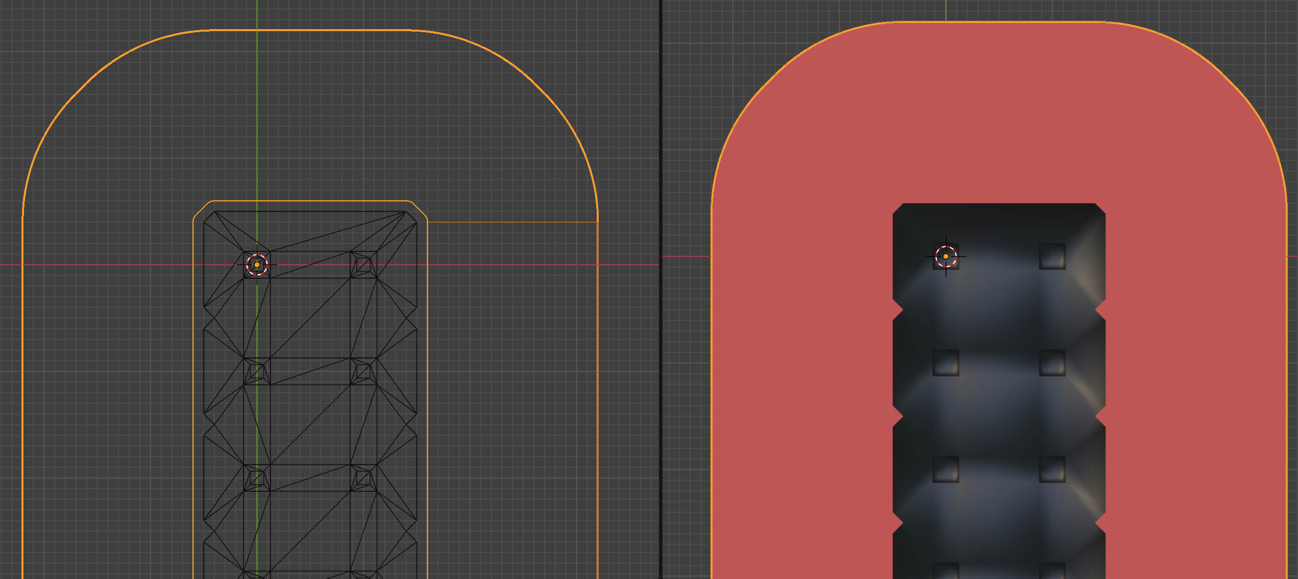
 Essentially images above show a 1.6 mm shelll, precisely 0.1 mm away from the berg header, placed at the exact location of the component derived from the board file.
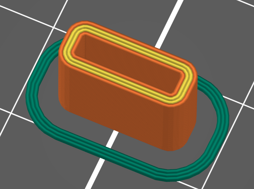
How will this work ? For a start, we can load the PCB design in KiCAD, find components, get to their 3D models, compute such structures using the meshes. Finally, assemble them all together, account for height differences and integrate them with the outline of the PCB with a neat slot for the PCB to fit. Many ideas running in my head - including avoiding connectors, securely attaching the PCB while soldering, ensuring the components fit snug on the bottom side, etc. I am sure there are plenty anybody else who needs a tool like this will come up with.
The idea sitting in my head for a day lead me to understand various possibilities.
What could one do with a full blown implementation ?
- Accurately assemble through hole components on a PCB (Goal #1)
- Component holders for GridFinity :) Yeah, totally snug fits!
- Faster SMD soldering for chips such as SOIC without fiddling with tweezers and such
- Automate case building maybe ?!
- PCB testing jig!
At this point, I say, stop! This is useful. Start a new project!
Discussions
Become a Hackaday.io Member
Create an account to leave a comment. Already have an account? Log In.