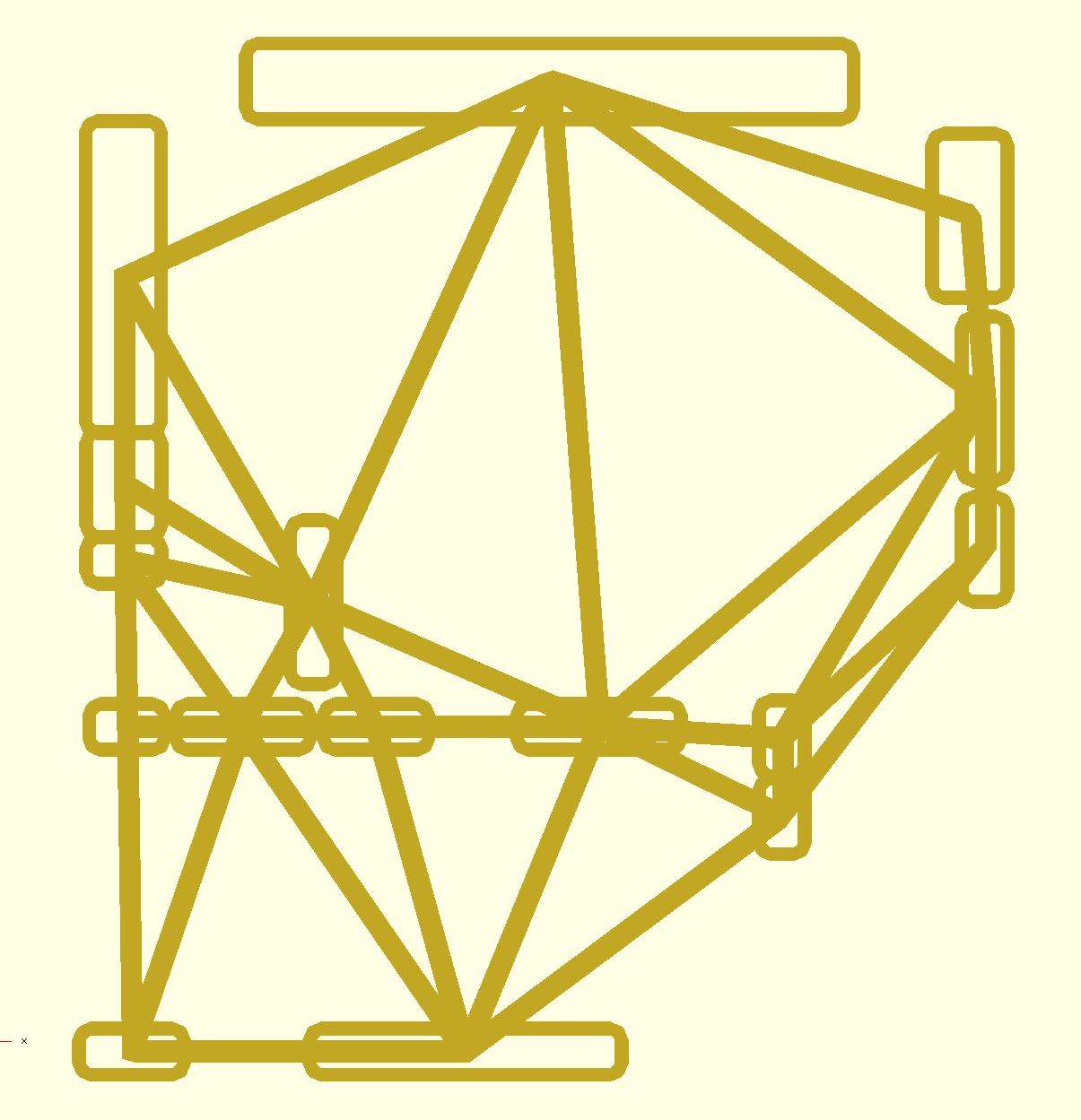
In the last log, I showed how the "shells" - or holders for each TH component are created. These shells need to be linked. It wasn't hard to figure out a way to do it. Anyone familiar with the 3D printing has seen the cool vornoi shapes, and probably heard the term "delaunay" triangulation. Basically, this computes a set of triangles linking a set of points. We can use the centers of each of the shells as the points, and we'll get a mesh. Simple to do in OpenSCAD.

The "base" of the components have to be solid of course - the image above hides them to show that the centers are linked together. The delaunay mesh gives us a few benefits:
- it saves plastic, directly resulting in a cost saving both of time and material. For reference, the typical thing people do when the create manual jigs is add a solid base plate - which obviously takes more plastic and thus time to print.
- it gives us a reasonably solid structure
- it enhances the visibility of the components, when they are inserted in the printed jig. If the plastic hits something - e.g. a component you've already assembled - it easy to see exactly what's going wrong.
Here is what the resulting structure would look like - when it is placed relative to the assembled board:

In today's development, I also ensured that the shells don't extend all the way to the PCB. In my board, I had a few SMD components close to the throughhole parts - e.g., near the RPi connector, there were some pull-up resistors. When the shells are built, their 1.2mm thichness intersects the SMD component. By not extending the shell all the way till the PCB, we can avoid this. This also gives me extra visibility into a side view of the components. When I eventually place the components and the actual PCB, I will be able to see and verify for myself that all the components are in fact sitting flush with the PCB. Here is what your view would look like, from the side:

So, this is getting exciting as it builds up. Fingers itching to print again, but delaying gratification for now one more time. The next step would be to import the outline of the PCB ('edge cuts' layer), and link it to this model. Lot of materials available on this - as many have built jigs to hold PCBs in place, holding stencils in place for SMD paste application etc.
 Shree Kumar
Discussions
Become a Hackaday.io Member
Create an account to leave a comment. Already have an account? Log In.