 Yann Guidon / YGDES
The currently used PEAC16x2 scrambler is nice but has two weaknesses :
- sub-par mixing
- the "mark" bits are too dependent on the input data
This was already considered back in 170. TODO: scan and elaborated with 1. Let's start.
The solution : a gPEAC chosen for its MSB and LSB.
Ideally, a "perfect" modulus should be chosen but the LSB are always 10. It was considered as a problem, since I wanted to reduce the size of the extra constant adder, so a string of 0s would have been great (or 1s...)
The new strategy is to reuse the existing adder and include the constant as a simplified MUX at the operands. The corresponding register gets updated only if a carry is generated.
The modulus could be "pipelined" with the data input but this would work only for one half of the circuit.
The adder is one thing, but the additional carry adds even more complexity. Actually, it's a delay for the C flag... so OK.
Let's return to the scrambler:

This version uses the simpler, binary PEAC with a typical power-of-two addition.
The non-power-of-two modulo requires a subtraction. Well, fortunately it's a constant value that can be easily encoded with OR and ANDN gates.
Now let's have two phases : one if "normal operation" (as described above), the second is "modulo".
- on the first phase, SumX goes to a register : there is a path to Y.
- on the 2nd phase, Y gets adjusted (on the SumY adder ?) but there is no direct way to loop it back without overwriting X.
So a new, more flexible, datapath is required with more MUX.
Design rule : avoid MUX (or other wide fanout signals) right at the output of the DFF because the fanout increases the latency.
However the "phase" signal could be relatively easily pre-amplified.
So let's start with the X and Y registers and let's go backwards.
Feeding X and Y are the MUXes, each with one constant and the output of one adder. Now this needs to be extended to the 2 adders. The MUXes now serve as a "swap" gate. Each register has an individual "write enable" signal, which could be implemented as another MUX but it's usually implemented within the DFF gate so let's just ignore this for the moment.

Extending from there, the datapath looks like that now:
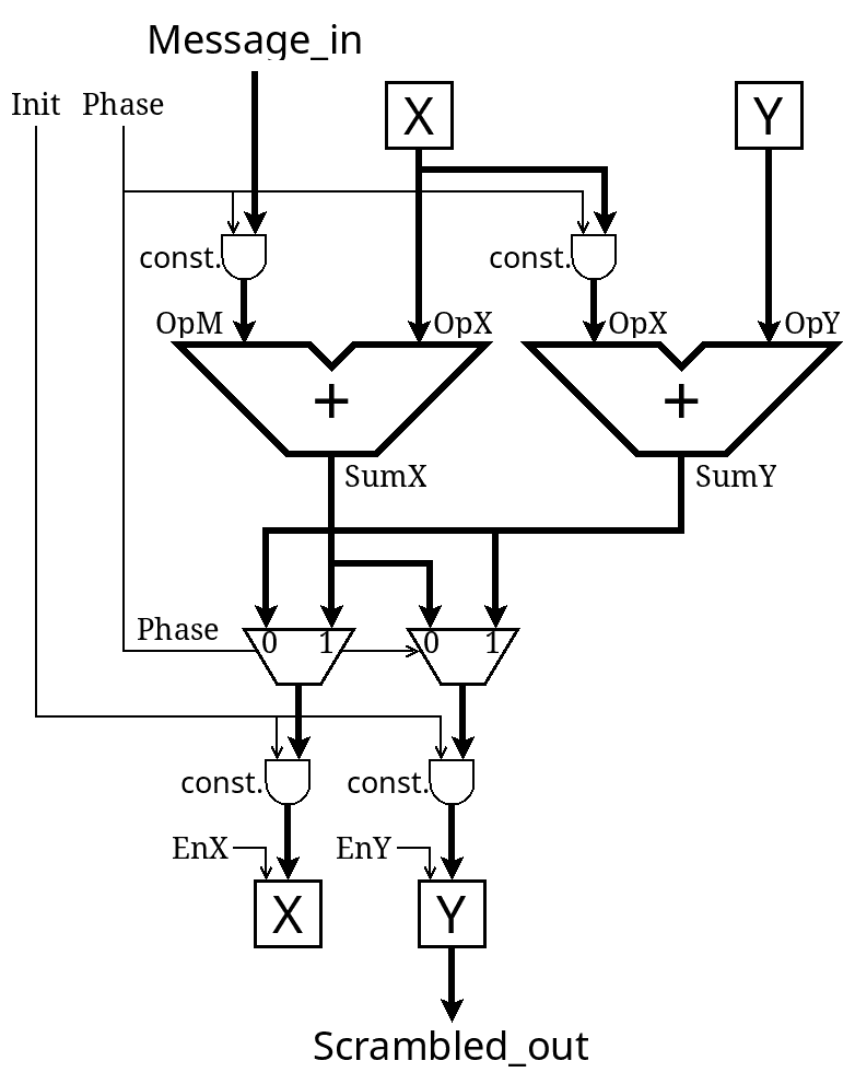
So each adder can write to either register as needed :
- Phase 0 : SumX writes to Y and SumY writes to X (actual computation)
- Phase 1 : SumX writes to X and SumY writes to Y (modulo adjustment)
The diagram is incomplete (no C & D registers)
One trick affects the order and assignation of the registers: the conditional write to the registers during the modulo operation. This makes the scrambled output valid only during Phase 1... But the word can be taken as a whole : the 18 bits are a valid scrambled code with marker MSB (no carry combination).
Next challenge : define the new constants.
Discussions
Become a Hackaday.io Member
Create an account to leave a comment. Already have an account? Log In.