Close
0%
0%

Hidden HID: an almost invisible Bad USB

maybe the worlds smallest (and least practical!) rubber ducky

Similar projects worth following
Edit 19.01.25: please have a look at the v2 page where I will be posting future updates :)
https://hackaday.io/project/202218-hidden-hid-v2-worlds-smallest-rubber-ducky

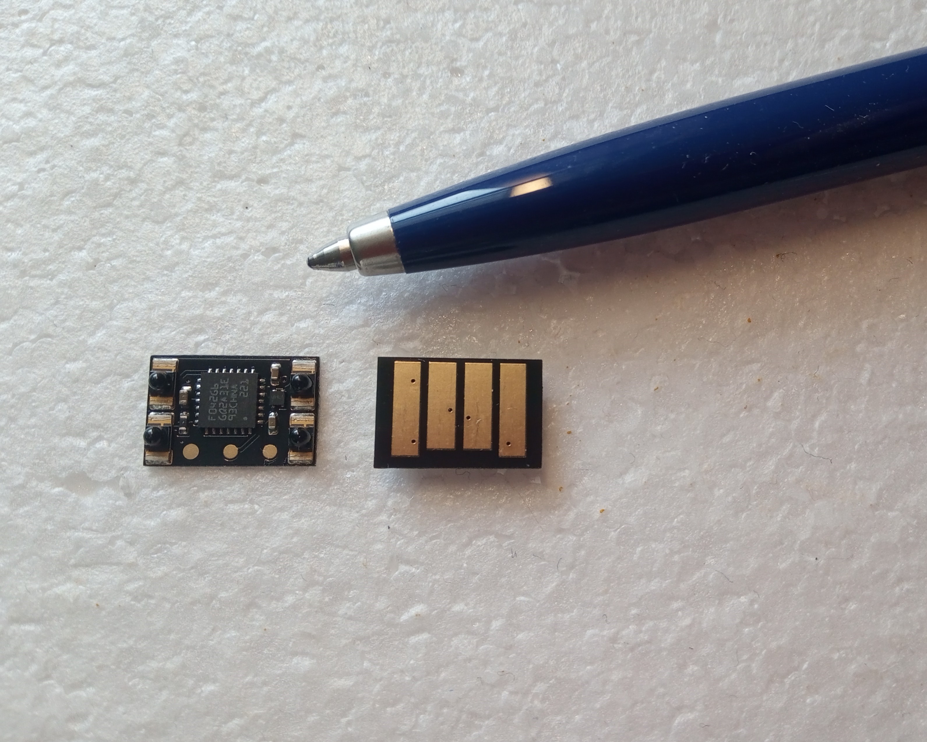
Hidden HID is a proof-of-concept demonstrating a tiny 8x12mm USB device that fits entirely inside a computer's USB-A port. While not completely invisible, it is unlikely to be noticed by anyone who is not expecting it --unless of course, they try to stick something else into the USB port ;)

In its current form, it presents itself to the computer as a mouse and pranks the unsuspecting victim by making the cursor jump around every few minutes.

In the next phase of the project, I will adapt the firmware to present as a keyboard, creating a tiny rubber ducky that can execute malicious code on the host PC

Thanks to PCBWay for manufacturing and assembling the PCBs!

Background

While researching PCB-based USB connectors, it occurred to me that there is quite a lot of empty space inside a USB-A port - around 12x8x2.5mm in fact! This is more than enough to accommodate a small microcontroller and associated components. And so the idea of Hidden HID was born - a USB device that fits entirely inside the port, with the components on the bottom side of the PCB, opposite the contacts.
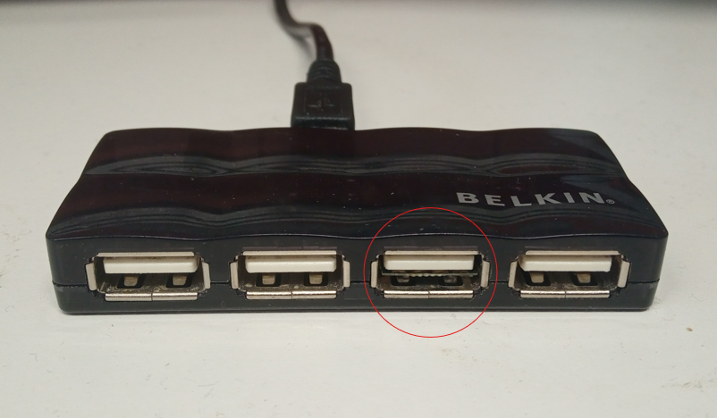
USB hub with the Hidden HID device inserted in the third port from the left
3D model of PCB inside a USB A receptacle

Read more »

  • 1 × STM32F042G6U6 ARM Cortex-M0 Microcontroller with USB interface 32kB flash in UFQFPN-28 package
  • 1 × NCP115AMX330TCG 3.3V fixed LDO in 1x1mm XDFN-4 package
  • 3 × XZM2DG55W-3 LED 1206 1.8mm high as mechanical spacer

  • V2 is here!

    Emma3 days ago 0 comments

    I have decided to make a new project to document the v2 PCBs and firmware - check it out here: https://hackaday.io/project/202218-hidden-hid-v2-worlds-smallest-rubber-ducky

    I will be changing the status of this project to completed, future updates can be found on the v2 page

  • PCB revision 2

    Emma11/28/2024 at 17:38 0 comments

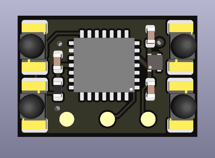
    3D model of PCB revision 2; bottom side. The three test pads at the front are the GND, BOOT0 and 3V3 pins respectively
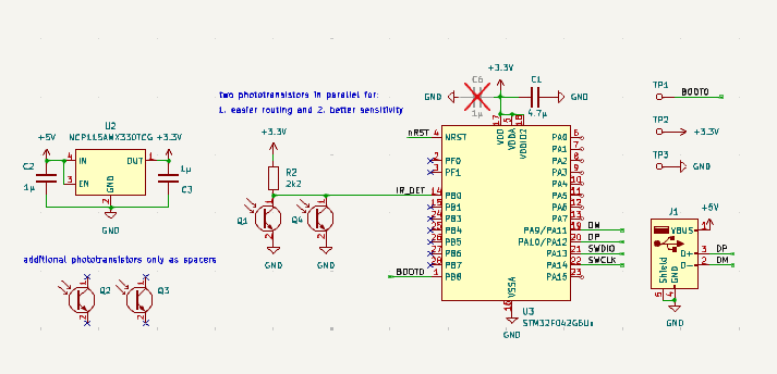
    Schematic of PCB revision 2

    While testing the first PCB revision, I identified a number of issues which I intend to improve in a second hardware revision. 

    1. The current version is very irritating to program. Due to the tiny size there was no room for any kind of connector or even a simple pin header. Instead, I simply routed the SWD and power pins to SMD test points with a diameter of 1mm. To program, I must then painstakingly attach the ST-Link programmer using magnet wire soldered to the test points, which then needs to be removed again to test the new application. This is ok if the device only needs to be programmed once, however flexible and easy reprogramming is a fundamental requirement of a USB rubber ducky.

      I had originally intended to solve this problem by writing a USB bootloader, but have since discarded this approach in favour of utilizing the preprogrammed ST USB bootloader. This has the advantage that I do not need to dedicate valuable program memory to my own bootloader. Furthermore, as the ST bootloader comes preprogrammed, I do not need the SWD interface at all, not even for initial bootloader programming. This allows me to simplify the layout considerably as the SWD pins no longer need to be routed to test points. The bootloader can be selected by tieing just one pin, BOOT0, high, and the PCB can then be programmed the same way it is used; by sticking it in the USB port.

    2.  The USB connection is unreliable. 9 times out of 10 the device makes contact with the USB port and everything works fine. Unfortunately, sometimes the board tilts very slightly to one side, leaving one or more USB contacts unconnected. I believe this is due to the fact that I soldered the spacer LEDs myself, as opposed to leaving it to the PCB assembler, and had uneven numbers of LEDs on each side, resulting in a slight height discrepancy. Now that I have established the optimal LED positions, I can try 2 LEDs on each side, adjust the layout accordingly and have them soldered by PCBWay, who will surely do a better job ;) 
    3. As previously mentioned, I would like to implement a simple remote on/off control by replacing the LEDs with IR phototransistors. I chose to replace all LEDs with the 1541201NC3060 phototransistor from Würth, which is a similar size and height. With the SWD test points removed, I had a little more routing space to play with and was able to route the collectors of 2 of these phototransistors to an ADC pin. The other two remain simple unconnected mechanical components as I found no way to route them to the pin. This part of the circuit is untested; hopefully it will be sensitive enough

    I have implemented these changes in the schematic and layout and sent the gerbers off to PCBWay for manufacturing and assembly. Now I just need to sit back and wait until they arrive :)

View all 2 project logs

Enjoy this project?

Share

Discussions

Carl Frega wrote 10/29/2024 at 14:47 point

Any chance of getting the Gerbers/etc?

  Are you sure? yes | no

Emma wrote 10/29/2024 at 18:01 point

updated with github link :)

  Are you sure? yes | no

Similar Projects

Does this project spark your interest?

Become a member to follow this project and never miss any updates