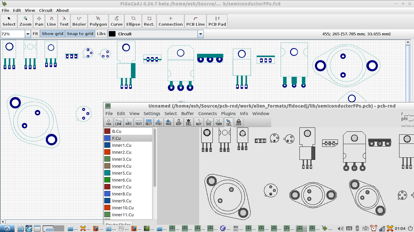
The text is behaving pretty well with round trip testing pcb-rnd -> FidoCadJ -> pcb-rnd

and footprints have been improved with circle, silk rectangle and minimum line thicknesses for silk elements

If all goes well, there should be some FidoCadJ equivalent footprints on gedasymbols.org soon....
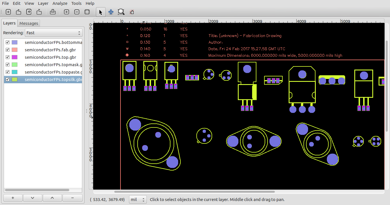
And here's an example gerber output of the Semiconductor footprints....

Discussions
Become a Hackaday.io Member
Create an account to leave a comment. Already have an account? Log In.