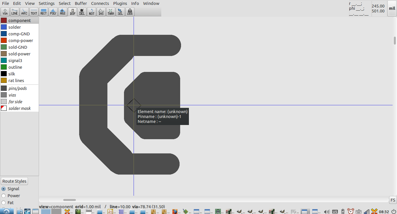
I've made a solderable link footprint in pcb-rnd, and will add them to the revised layout for the three LED power distribution networks. This will simplify programming as well as testing after assembly.
I think I'll add support for the solderable link footprint as a paremtrically defined element; it only needs a simple awk script and glue code.
I might also add pads for a resistive divider so that the ADC on the spare pin can figure out what speed to flash at, so that one lot of code can be used for FSMs flashing at different rates, simply configured during construction with the right resistor network.

Discussions
Become a Hackaday.io Member
Create an account to leave a comment. Already have an account? Log In.