Hiya, folks.
So, I've been rather interested in low power stuff recently and I needed a good way to generate 3.3v from a single or dual AA-battery with good load efficiency at lowish currents. Additionally, as this was for a futre-to-be-determined battery powered project, I really wanted to keep the quiescent currents as low as possible for extended battery life. Finally, as a "just because", I wanted to use a single power button for on/off control and a way for a microcontroller, or whatever else, to kill the system power if needed.
This is just a small sub-circuit of a larger project that I'm considering.
Here is the schematic:
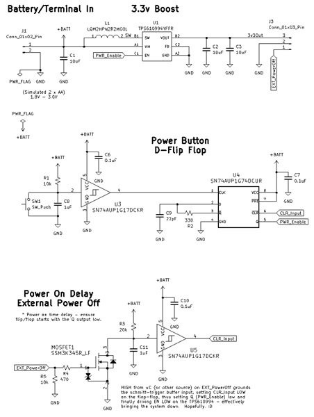
Regarding the button power latch, there are numerous schematics/examples floating around the internet utilizing discreet components and a pair of mosfets or bjt's. Oddly, there are even a handful using a 555 (!). However, I wanted to go the D flip flop route as there are a lot fewer examples of this (that I could find) and it just seemed more appealing to me.
I understand that the inclusion of the buffers may seem like a bit of overkill, but I like my signals tight, probably to a fault. :D Regarding the buffer (U3) for the clock input of the flip flop, a clean HIGH and LOW signal transition seemed especially relevant. Additionally, the button bounce problem is completely eliminated in this way as well.
I can argue that the buffer for the power on delay (U5) is especially overkill as I'd be pretty darned certain a simple RC timing-circuit would be all that is needed here. To further support the removal is the fact that it really only comes into play when batteries are first installed or otherwise swapped out -- it's not doing much of anything otherwise.
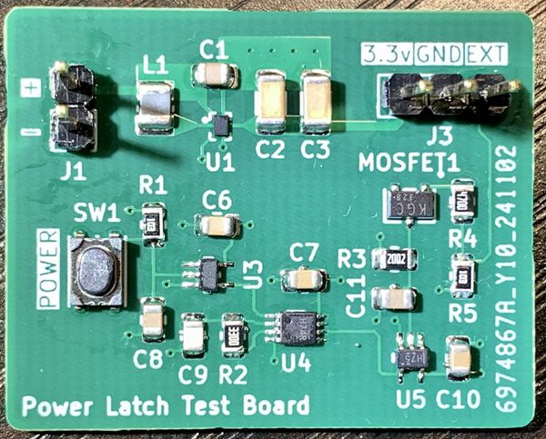
Here is an image of the test board:
And layout:
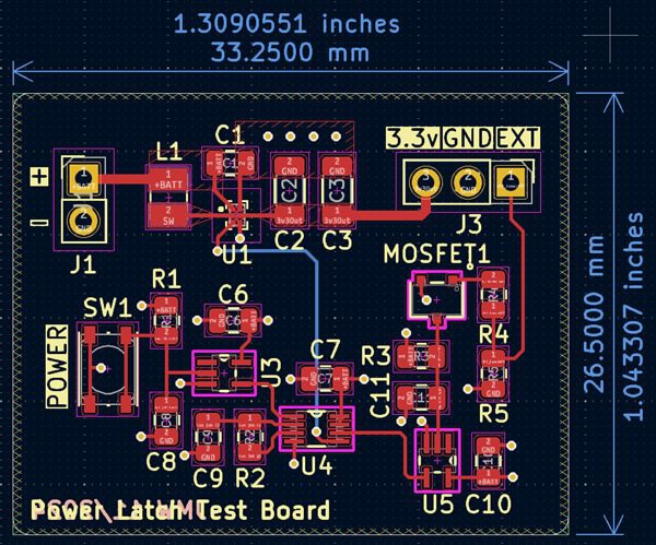
I did realize that I need to pay A LOT more attention to datasheets -- when I was part-picking and found the boost converter, I didn't realize the size of the darned thing. After ordering the parts and finishing the schematic, I only discovered my error on layout... this thing is frighteningly tiny -- 1.23 mm × 0.88 mm.
Below is a close-up of the power section. For reference, C1 is an 0805 and the output capacitors C2/C3 are 1206's... the little 6-BGA is about the size of a single pad of an 0805. I will not make this mistake again, that's for sure.
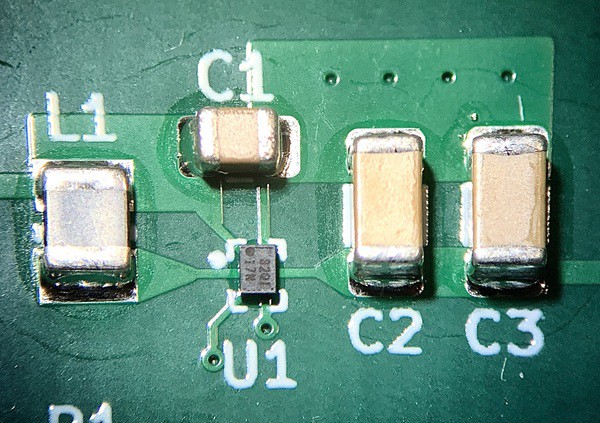
The layout of this section is pretty much a carbon copy of the suggested layout in the datasheet on page 19. In the next revision, I'll definitely try and tighten things up a bit more as well.
At any rate, I'm just happy nothing burned up on the first test power up. Did a bit of power profiling on it and I'm very happy with the idle measurements. With the downstream power off (TPS610994 EN LOW), the board pulls about 0.64 uA, which is awesome.
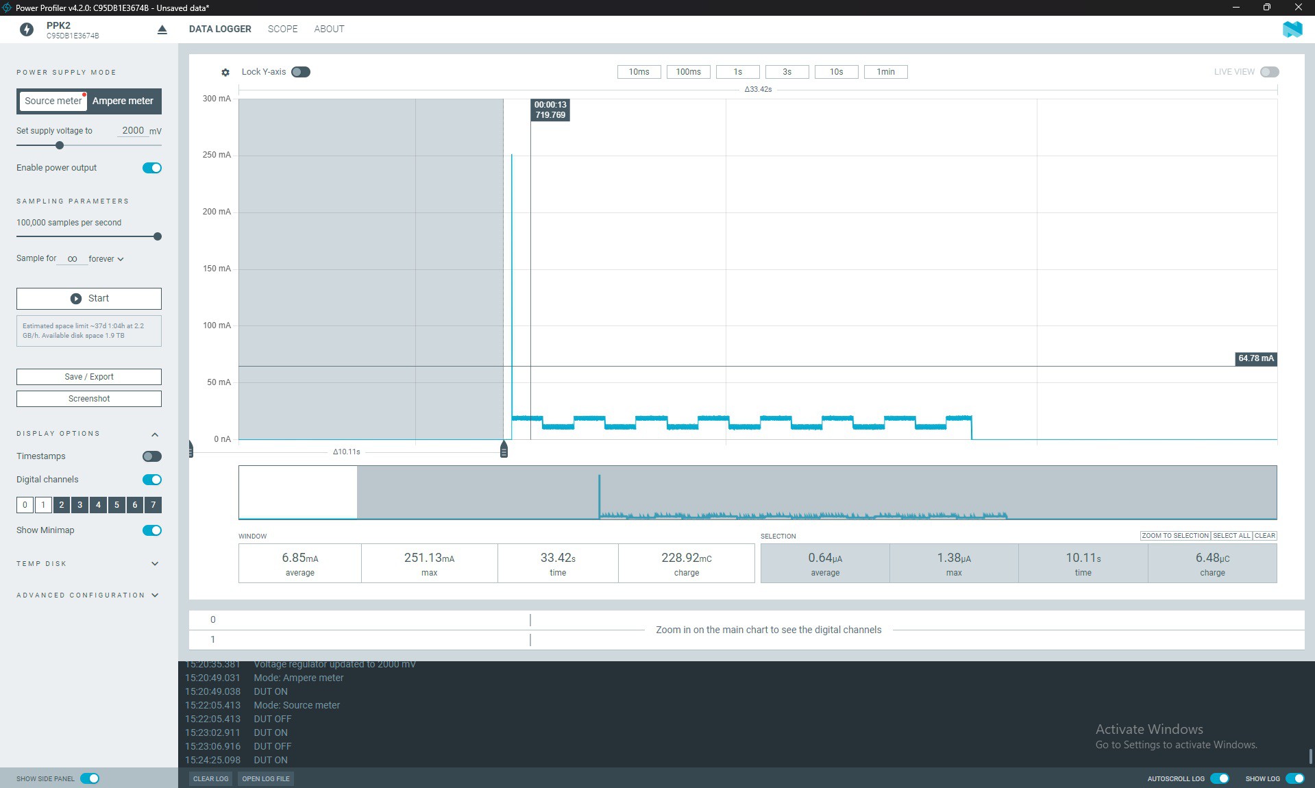
A small test load consisting of a STM32G070KBT6 blinking an LED was used for the power-on testing. The large spike at power-on is more-than-likely inrush current from the two output capacitors of the boost converter and the caps for the STM32.
Overall, I'm quite pleased with this... expectations were fully met, and it was fun, which is the best part.
 AccidentalRebel
 Stefan Kratz
 megahercas6
 Nick Sayer