WITCH-E Decimal Based Computer
Document and create a modern replica of the Harwell Dekatron computer known as the WITCH
Document and create a modern replica of the Harwell Dekatron computer known as the WITCH
To make the experience fit your profile, pick a username and tell us what interests you.
We found and based on your interests.
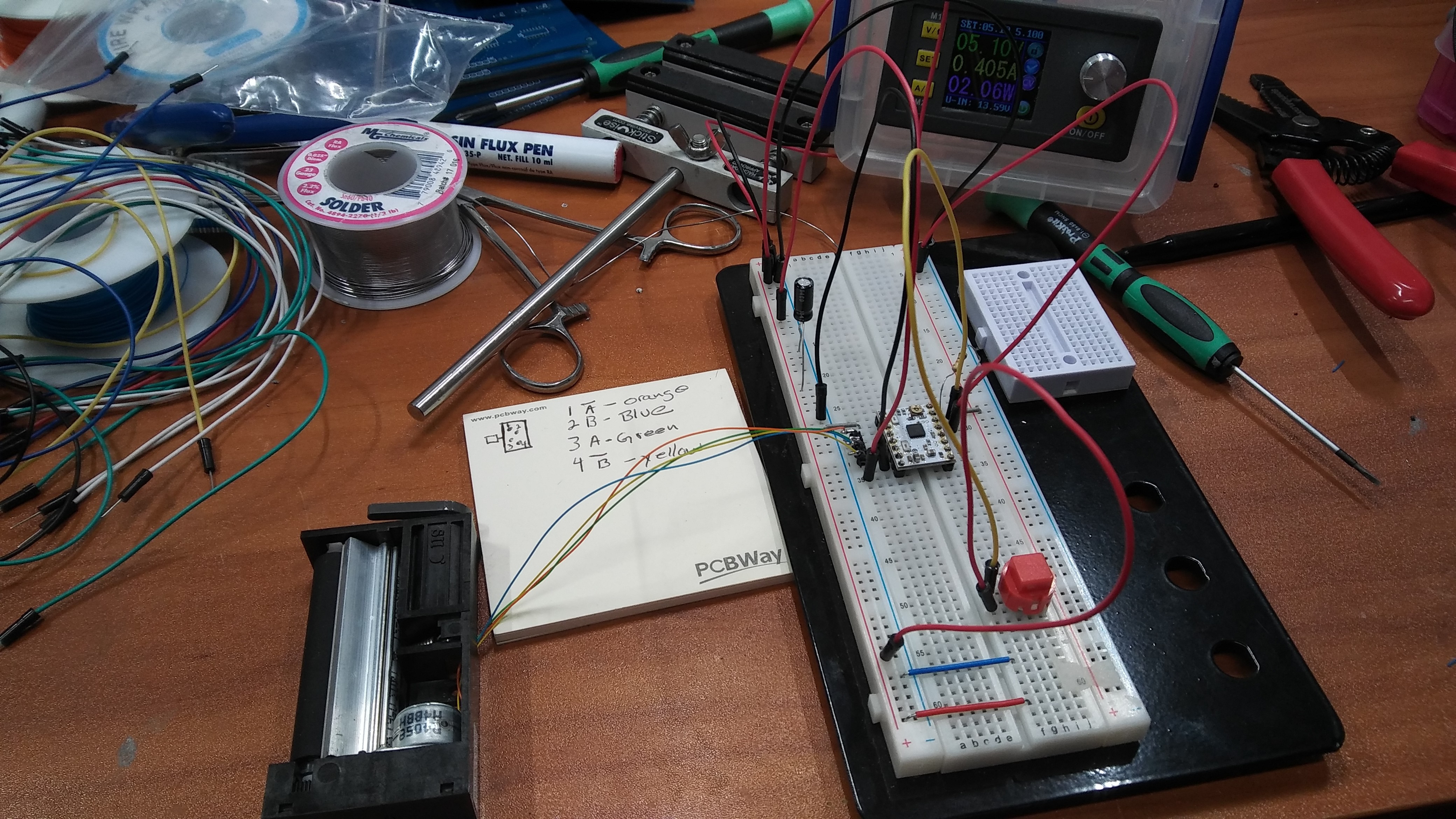
After getting Phase3 working with the 5-wire input system, the next step is Phase4 with the paper tape reader. I've not completed Phase3 yet, but I am close, so it's time to start doing some more prep-work for Phase4. I got a 3" (80mm) printer assembly off ebay a couple weeks ago. There are a number of these printer assemblies available as replacement parts. The one I select for testing is the Seiko LTP1245, which has a ton of clones available. It has a 5V 2-phase stepper motor that drives the pinch wheel for the paper. I found the Texas Instruments DRV8834 during some basic searches and it looked perfect for interfacing with my simple circuitry replication from the original tape reader interface on the WITCH. After a couple quick google searches for a breakout board for the DRV8834, I found one from Pololu that looked perfect for testing. Of course, for Phase4 of WITCH-E, I'll be designing my own boards for this, but during prototyping and testing this makes it super easy. One of the concerns in selecting a driver chip was that it was available in several packages. While I do have resources to work with QFN (Quad Flatpack Noleads) packages, I'd prefer to have something easier to solder by hand, and the DRV8834 is available in 24HTSSOP which I can easily solder by hand. Get to stepping!
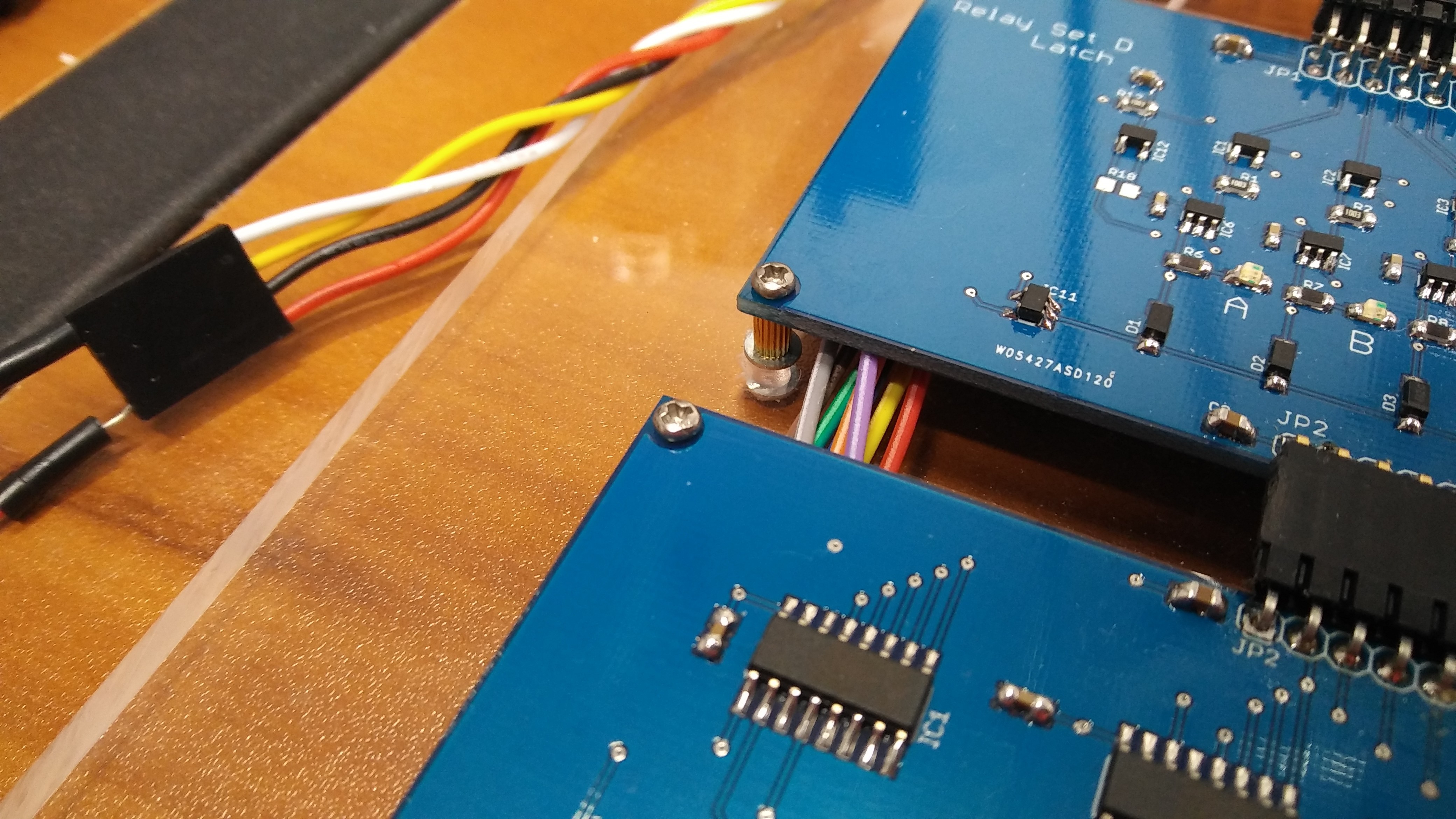
During this phase of integration, I recently built up the first of the Relay-Set-D Decoder boards (Half-Ass Assembly...). I took some time this evening to place one on the temporary acrylic and mate it with the Relay-Set-D Latch board. Immediately I was in a state of total panic.... yes the edges of the PCBs did not align!!! ZOMG!!!! Going back to the PCB layout design files I realized that the connectors on the Relay-Set-D Decoder were 5mils off!! NOOOOOOOOOOOOOOOO....................... I am so triggered:
Must
Order
New
Boards
NOW!
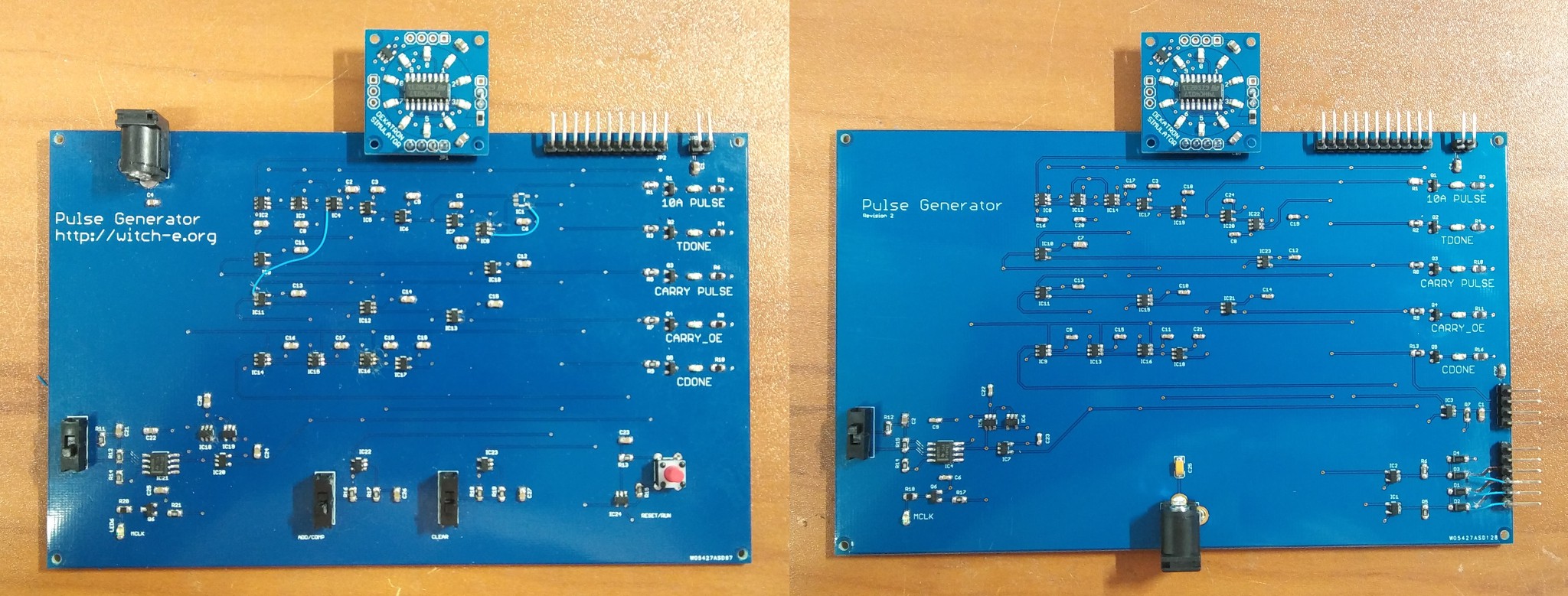
Got the new Pulse Generator assembled! The "new hotness" has the barrel jack moved as it was in an awkward place on the "Old Busted" design. I've removed the two switches and push button, replacing them with connections to the 5-wire input system. I also corrected two of the "white wire" changes that were required from the original design. Of course I am going to have to spin this design due to my "Off-By-One" error , and I really should have added some LEDs to indicate what function is being called, so this is technically "New Busted"... oh well....
As a side note, this PCB is 160mm x 100mm , and actually contains three separate sections. Most PCB shops will do quick turn prototypes pretty cheap if the design is 100mm x 100mm or smaller, so looking back on the design, it would have made more sense to break this up into at least two boards, and maybe three... it would have saved a lot of money and made the "logical module" appearance of the design better... 20/20 hindsight....
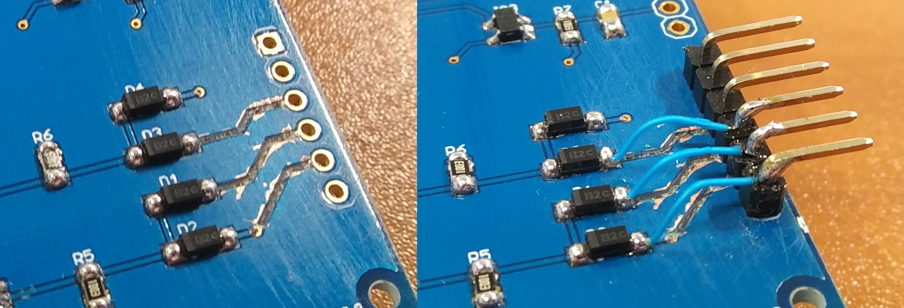
I ordered the new Pulse Generate a little over a week ago. It was due to arrive on Friday, but on Thursday night I woke up in the middle night in a state of panic that only Freddy Krueger could have generated. I just realized I had an "Off-By-One" error on the PCB for the Pulse Generator that would be arriving the next day. I HATE IT WHEN THIS HAPPENS! I found some time this evening to start the assembly of the Pulse Generator. One of the first items to address were the changes needed for my little mistake. I took an exacto knife and removed the three traces from the PCB. I personally like to remove the whole trace, one for the fact that it appeals to my OCD, and two as it gives me a strong visual clue that the board has been modified and exactly how it was modified. I carefully cut the trace on each end and then use the edge of the knife to pull up the trace. As you pull the trace up it will work back to connection point, and if you've scored it properly will stop there. There wasn't an "easy" way to add wire fixes for these traces so I just soldered them to the base of the connector. This connector has a lot of room at the base, so it won't interfere with the mating connector. This will teach me to order PCBs at 3am.... DOH!

Well.... sorta! The original WITCH computer ended up with 10 available storage locations, with each storage location having 10 addressable registers, however it didn't start that way. During the early prototype and development of the WITCH, there were only 3 storage locations available! With this in mind, I made similar design/prototype choices during Phase-2 of WITCH-E to only make 3 storage locations. Phase-2 also only supports four functions instead of the full 10 on the original WITCH. The four functions are: Add, Add with Clear, Subtraction, Subtraction with Clear. The Relay Set D Decode board needs to support the eventual capacity of all 10 storage locations so that is how I designed it, but at this stage, with only 4 functions, and 3 storage locations (with 4 registers each), there is no need to build up all of the support on the Decode board. I KNOW I will eventually have to make changes to the Decode board due to testing and debugging, so it just makes sense not to build up the full support and waste parts at this time.... Yeah... I know... it does look a little "Half-Ass" but hey, we can all try to be optimists and think of it as "room to expand"!
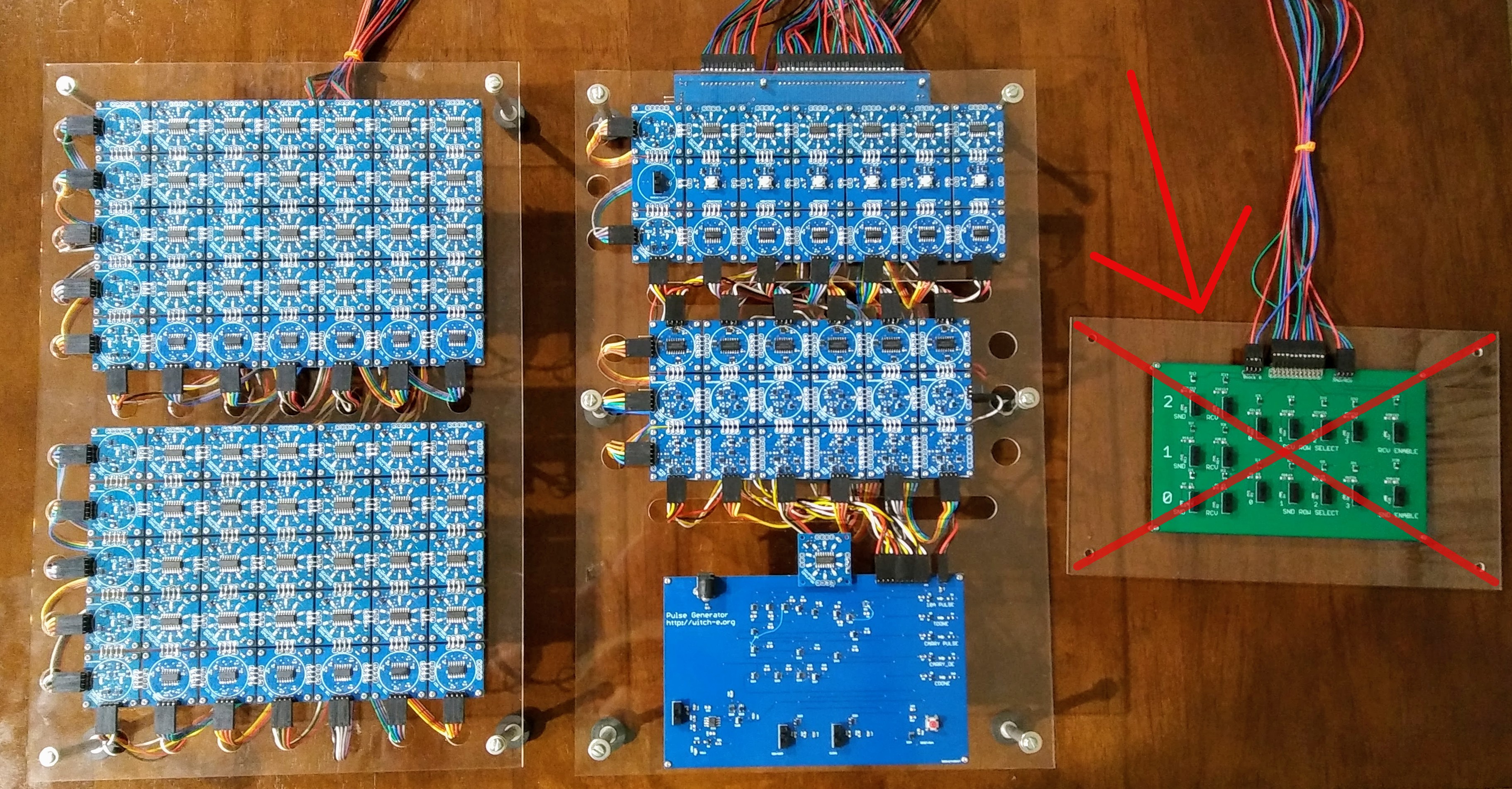
During Phase-2 of the project it was necessary to create a small test board to enable the various functions and memory locations. That board is the "green one" in the picture above. It basically consists of a number of switches that all each of the memory locations to be activated as well as select things like addition, subtraction, and clear functions. To bridge the work done in Phase-2 to the input system built in Phase-3, I need to replace the green test board with a bridge board that will connect the two development phases together. This basic board has some Schmitt triggers on it to clean up the signals from the long wires and then route the signals to separate connectors for each of the input system decoders. It's a super simple board, but it is essential to connecting the two sections together!
I had hoped that using a schmitt trigger and some large RC (Resistor/Capactor) values would have been enough to debounce the valid data and select signals, but it just wasn't the case. After reviewing the timing on the oscilloscope, I decided to prototype a monostable multivibrator with a 555. Now, I couldn't just use the standard circuit that is usually associated with a monostable 555 that is found on the net. The main issue is that if you have a timer set for 1 second, and you hold the trigger signal low for 2 seconds, the timer expires. What I needed was a timer to start AFTER the trigger is released. Of course, like most things in electronics there hundreds of ways to do this, but this is what I came up with. Now time to update the PCB layout...
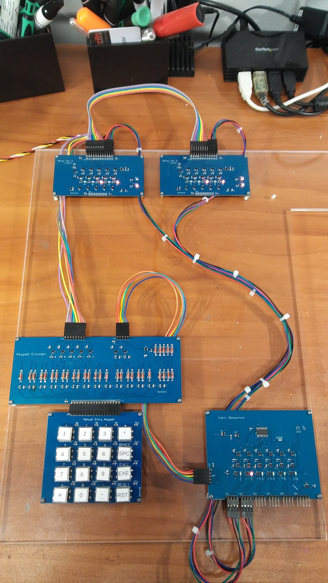
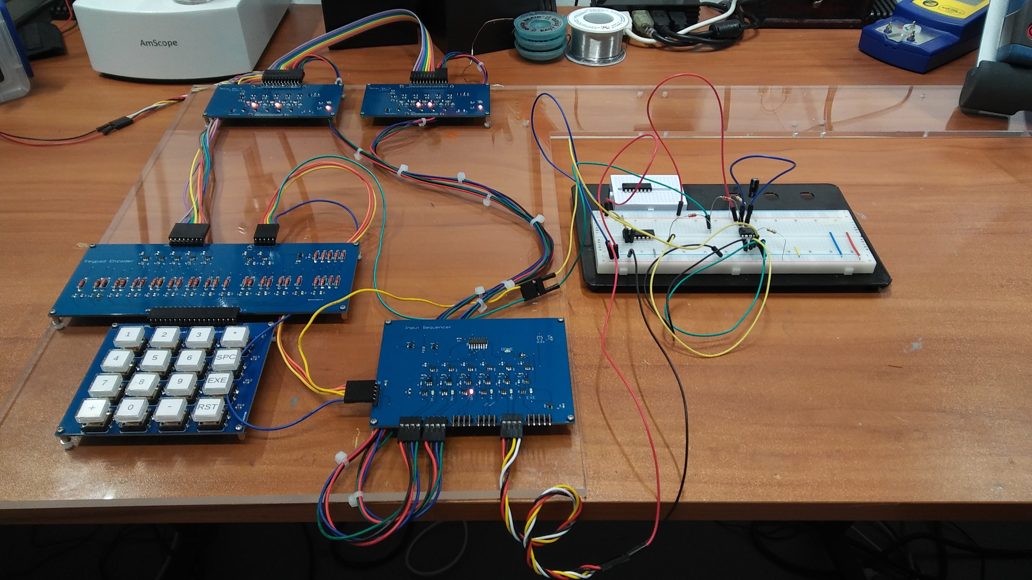
So I finish up extremely late this evening with my "DayJob", and despite being a bit a drained from debugging some new hardware all day, I decided to build up another Relay-D Latch board. I also found some scrap acrylic in the the garage and drilled some holes to mount the modules. I plan to get laser cut acrylic via Ponoko.com , but for now this will help test the cable routing and keep things from flopping around. I had to tweak the schmitt trigger RC values some to get the firs latch to work, but it eventual worked. Unfortunately, tweaking the RC values wasn't enough to keep the second latch from getting a carry over from the first latch. I'm going to have to work on my "key up" and debouncing before I do the next revision...
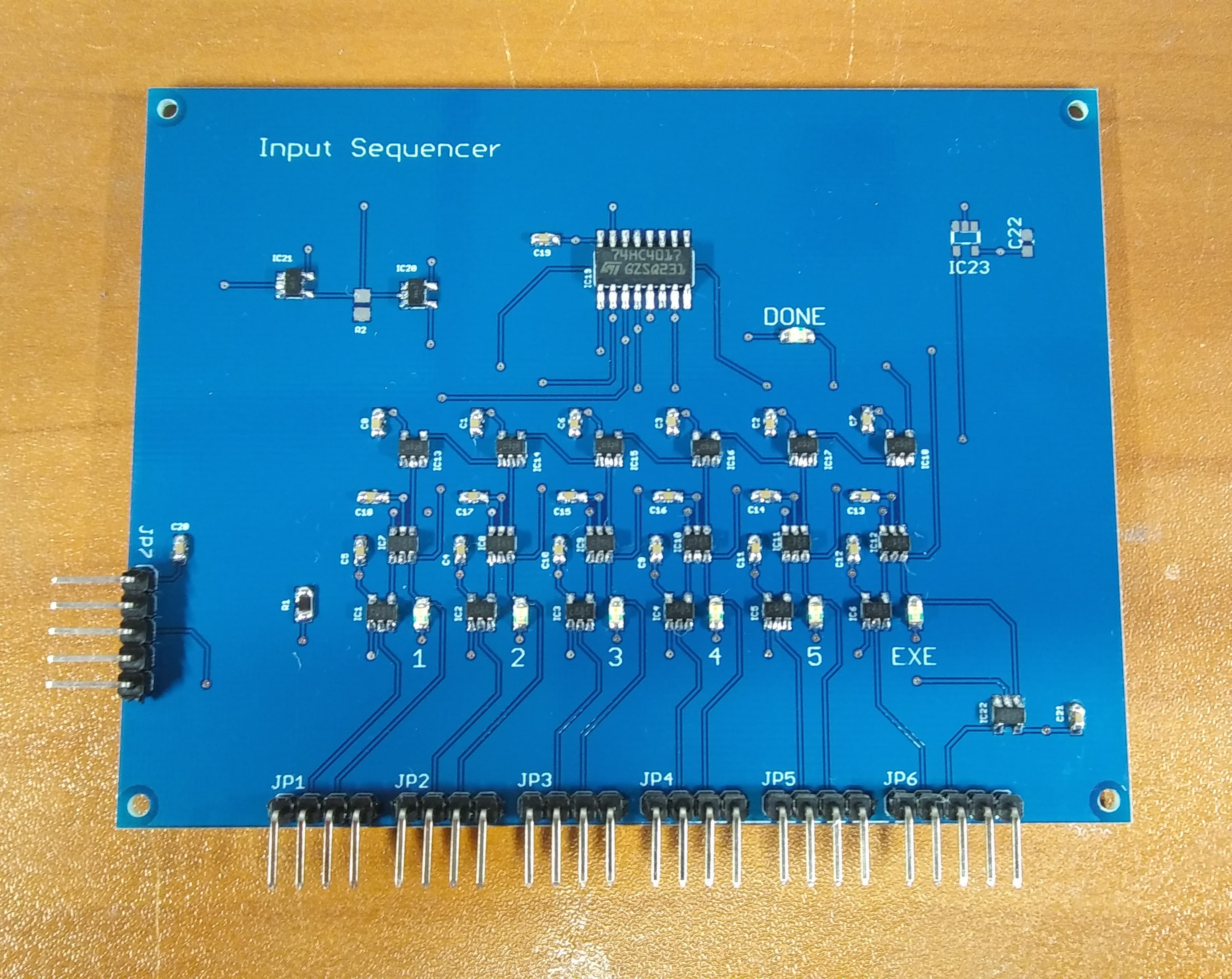
This new revision of the Input Sequencer board only had some minor changes to it. During my over-haul of the cabling and connections, I realized I needed to pass a few signals through the input sequencer. I also thought I might need an extra reset signal out to some of the modules, so I added a Schmitt trigger output, but not populating it until I actually need it. One think I might change in a feature revision is the decade counter. Right now I am just using a standard 4017 chip, but for looks, I think I replace it with a Dekatron Sim, like I did on the pulse generator module. Next step is to build up the Relay-D Latch boards....

So my daughter was off to work and stopped by my office. She saw that I was experimenting with different cable routing paths, so she took a few minutes to draw a block diagram. For this phase of the project, there are 4 large sections of laser cut acrylic that would hold each of the modules. I was struggling to see how I could mount all the modules and get them connected. I really see the challenge of the early computer developers on how to route and connect all these modules together. Before Integrated Circuits (ICs), this was often referred to as the "Tyranny of Numbers". How do you exactly plan for the massive number of wiring connections between modules and make sure that the minimum number of necessary connections are made. It takes a completely different way of thinking to do this. The really scary part of this log post is that there was very little I had to explain to my daughter. She "just drew" this with little guidance, and I am thinking "wow! did I really inadvertently ruin my children with my nerdy projects?" Maybe... but at least she can laugh knowing that she is fully aware of how to use a soldering iron and can point out the obvious to other people.... ouch! Smells like chicken!
Create an account to leave a comment. Already have an account? Log In.
If this was available as a kit, with through-hole components... I tell you what, I'd be saving every penny I could, for one. This is awesome.
thanks for the feedback! i had originally planned to do the entire design with through hole components, but after talking to a few people decided there probably wasn't going to be enough interest in a kit, so i went with SMT components as it allowed me to make the design a bit smaller...
Just out of curiosity, how much would it cost to produce a full build, assuming PTH components?
for a full build, pcbs,components, cabling and such, unassembled, probably around $800 to $1200. the main issue is the volume of course... over the course of the last 7 years, i've spent a little over $20k doing prototypes, testing, and equipment purchases on the design... it's really starting to come together this year!
Yea, there are a lot of components in the design! i have been thinking about your request. a smaller version that would be less modular, and use a USB interface for the tape/data entry, could be possibly made for around $200 to $300. i'm going to look more into that in the next few weeks...
12mm tact switches and switch caps are cheap on eBay's HK side ;) and the white square caps with clear covers you can get would be perfect for a keyboard for something like this... label the caps with eg an Ultra Fine Point Sharpie, add a cover, plastic might yellow eventually, but that label will never wear off. Caps are $9.85 for a hundred from the one seller that currently has them outside of assortments -- 'yayaya168' is their name. Lots of sellers have the corresponding tact switches, although they tend to come with /other/ caps... one seller has them $2.59 for 50, although you'll have to pay somewhat more if you want ePacket shipping...
...while I'm at it, orange 3mm LEDs (for the /slightly/ more authentic look) are about $8.50 for 500pcs, same source. That drops to $5, if you can stand red instead...
When you're flat broke like me, Mouser prices are a little too extravagant, so you learn to go other places ;) I'd probably get the 4017s from Mouser, though, just to eliminate that as a source of frustration. Not every seller on eBay is scrupulous enough to send you the right thing. I've heard of people getting mislabeled 7400s for example, instead of whatever /other/ 74xx chip they ordered...
yea trust me i am old-hat at BOM reduction, but there is more to it that just the components. i have get bags, shipping for parts, packing materials, pcbs and not to mention the cost of prototyping the changes. plus i wouldn't be doing it for my health... i would need to make some profit out of it. it us a lot different making product than just doing a one off project... i am still running the numbers and thinking about how i could make it into an educational kit..
All of this is true :) I was just providing a couple examples of how that $800-1200 could perhaps be lowered a little...
Really the problem with eBay part sources is reliability, both in terms of cost and in terms of what you get for that cost. It's almost rare for something to be the same price from the same seller twice, unless you're buying in rapid-fire fashion. That, and whether or not what you buy actually /works/ is always a question as well -- I would not want to be the one who gets to test all 500 of those LEDs ;)
yea the main issue is that it is intended to be a replica of the WITCH. this means there is a lot of 1:1 circuity that is replicated as part of the WITCH design that could be made easier with modern components. an example of this is the 5 wire input system. the WITCH (and my design) uses a 5-bit baudot code for the data input. the entire design could be simplified greatly for use with modern components by replacing this with standard 4-bit BCD encoding. that one simple change would reduce the cost by $150 easily....
indeed the design is using 74HC4017's to simulate the functionality of a Dekatron. I am currently on the 4th revision of the Dekatron Simulator in 6 years. this version has been optimized for easy assembly on a desktop pick and place machine. all of the designs are done in Eagle CAD and are release under the Creative Commons CC-BY-SA 4.0 license.
Become a member to follow this project and never miss any updates
 Tom Thoen
 Anderson Antunes
 jason.gullickson
hi we have decimal cpu an adder