Each Haasoscope Pro can sample up to 3.2 GS/s on a single 50 Ohm input. But to take advantage of the 2 GHz of analog bandwidth, we need at least 4 GS/s according to the sampling theorem and of course more is better. Fortunately, Haasoscopes are meant to be synchronized, and by combining two Haasoscope Pro's we can get double the sample rate, 6.4 GS/s. The idea of oversampling is just that the samples from one ADC are interleaved in time with the samples from the other. For example, if ADC1 is sampling at times 0ns, 1ns, 2ns, etc. then ADC2 samples the same signal at times 0.5ns, 1.5ns, 2.5ns, etc. Sounds easy, but we need to get the analog signal into the second ADC while maintaining sufficient bandwidth. And we also have to sample the signal in both ADCs at sufficiently accurate times, with sufficiently small jitter.
To get the analog input signal split off into the second Haasoscope Pro, we use a resistive power splitter. The input at port 1 on the left gets split using 3 resistors into the two ports on the right. The resistors just need to have resistance equal to the characteristic impedance of the inputs and outputs, which is 50 Ohm for us.
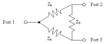
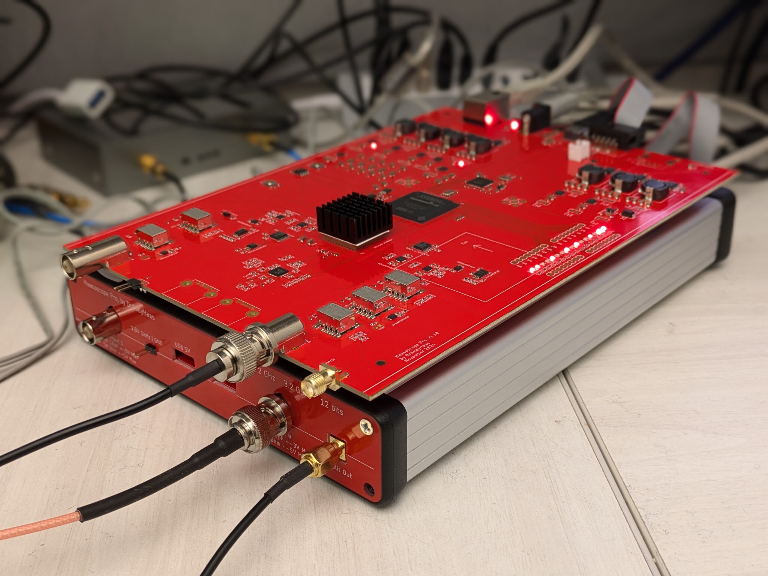
Actually, the input and outputs are all symmetric as you can see, so any one of them talks to the other two. This works great up to very large frequencies, limited only by the parasitic capacitances and inductance of the resistors. The outputs will each be 6 dB smaller in voltage than the input, so 1/4 of the input power. (Half of the power is wasted as heat in the resistors.) One output is sent to the ADC on the first board, and the second output is sent out to an SMA connector on the front panel. An external SMA to BNC 50 Ohm coaxial cable can then be used to get the signal to the input of the second Haasoscope Pro for sampling by its ADC.
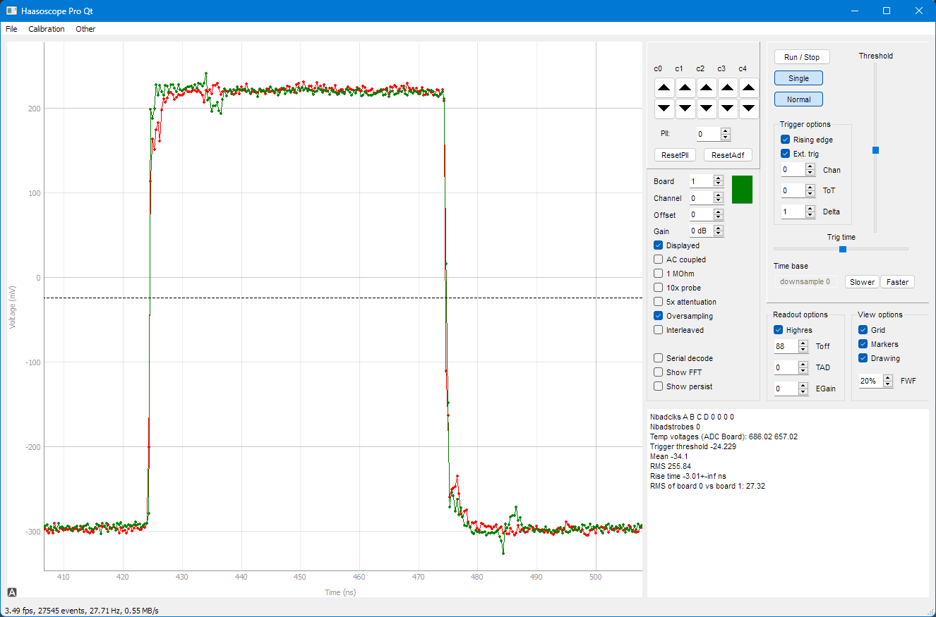
That basically works, as shown just below. The green is a signal sampled by the first board, and the red is the same signal triggered by the first board but sampled by the second board. Looks pretty good, but not great. The signal has degraded a bit by the time it gets to the second board, particularly at higher frequencies (close the sharp rising edge).
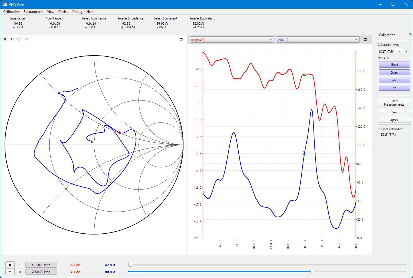
This is expected, since it had to go down more PCB traces, and through an extra SMA and BNC connector, and through a cable, all of which have more signal loss at higher frequencies. In fact, a NanoVNA V2 PLUS4 was used to test the frequency response of the whole splitting path. It's indeed down by about 2dB at 2 GHz compared to at low frequencies.
To recover these losses and make the two signals seen by the two units more similar, we need to allow more higher frequency signal through the splitter for the second output. The idea is to decrease the impedance of its nominally 50 Ohm resistor by adding a capacitance in parallel, whose impedance of course decreases as frequency increases. The relevant frequency where the parallel path will start to significantly impact the impedance is about 1/2piRC or about 400 MHz for 15pF, given the 25 Ohm relevant here in the splitter leg. The result looks like this (the red and green got switched I think):
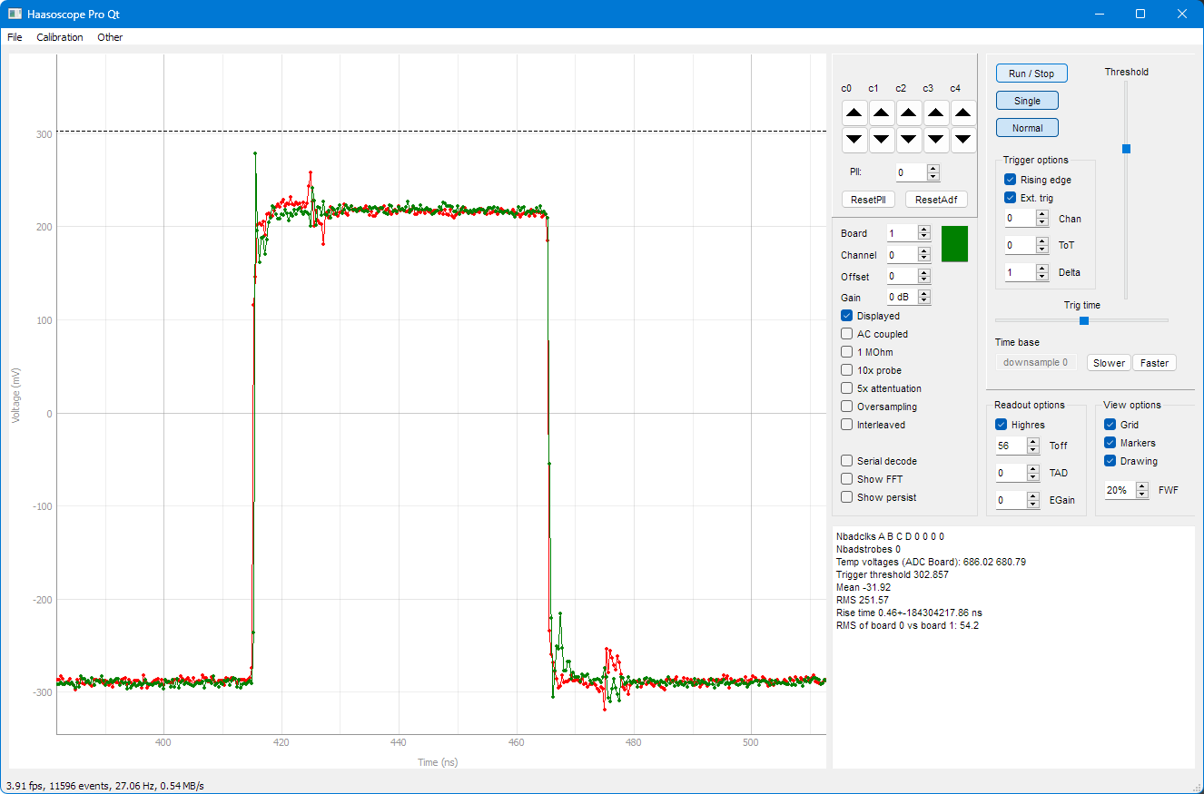
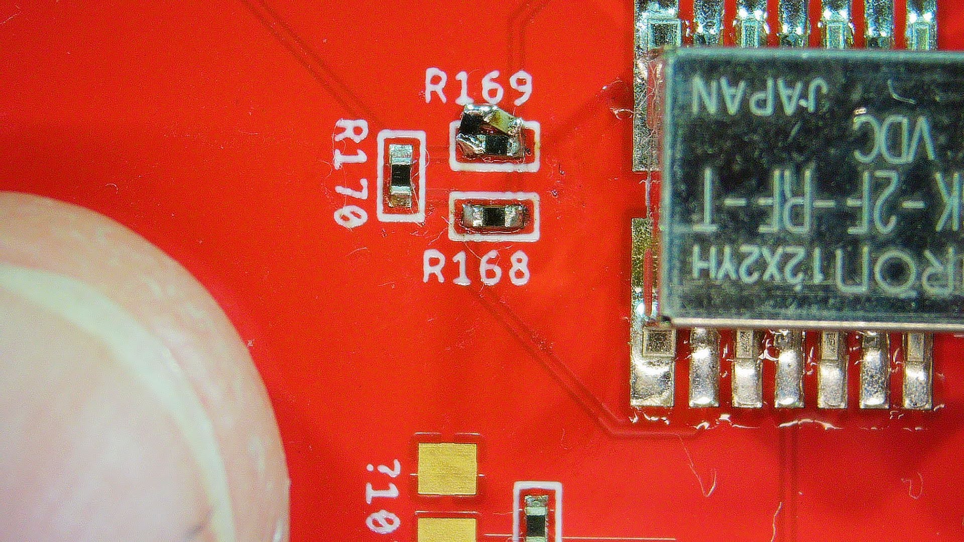
The green definitely is boosted at high frequency, but the issue is that the impedance now goes to zero at high frequency, so there's a big spike on the rising edge. What we need is some additional resistance on that parallel capacitor path, so when the impedance of the capacitor goes to zero, there's still the impedance of the resistor in series with it. This is what those 0402 components look like, with the tip of my finger for scale, hacked onto the board.
This is what it looks like with 15pF in series with 15 Ohm on the parallel path:
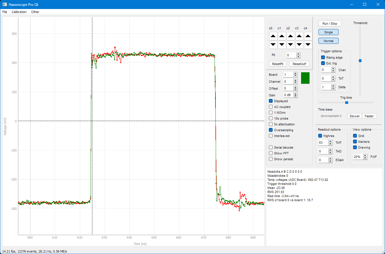
Much better! But it still dips down a little. Here's 27pF in series with 27 Ohm:
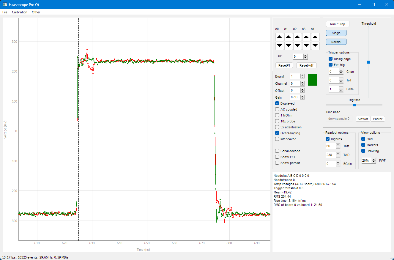
There's still a small remaining issue, which is the small reflection on the first board's signal (red), just after the rising (or falling) edge. That's coming from a small impedance mismatch between the cable and the SMA / BNC connectors I think. It moves in time depending on the length of the cable. Adjusting the termination impedance of the single-ended to differential amplifier, the LMH5401, from 357 Ohm (as recommended in the datasheet) to 220 Ohm seems to help. Here's what it looks like, after also changing to 16pF in series with 47 Ohm:
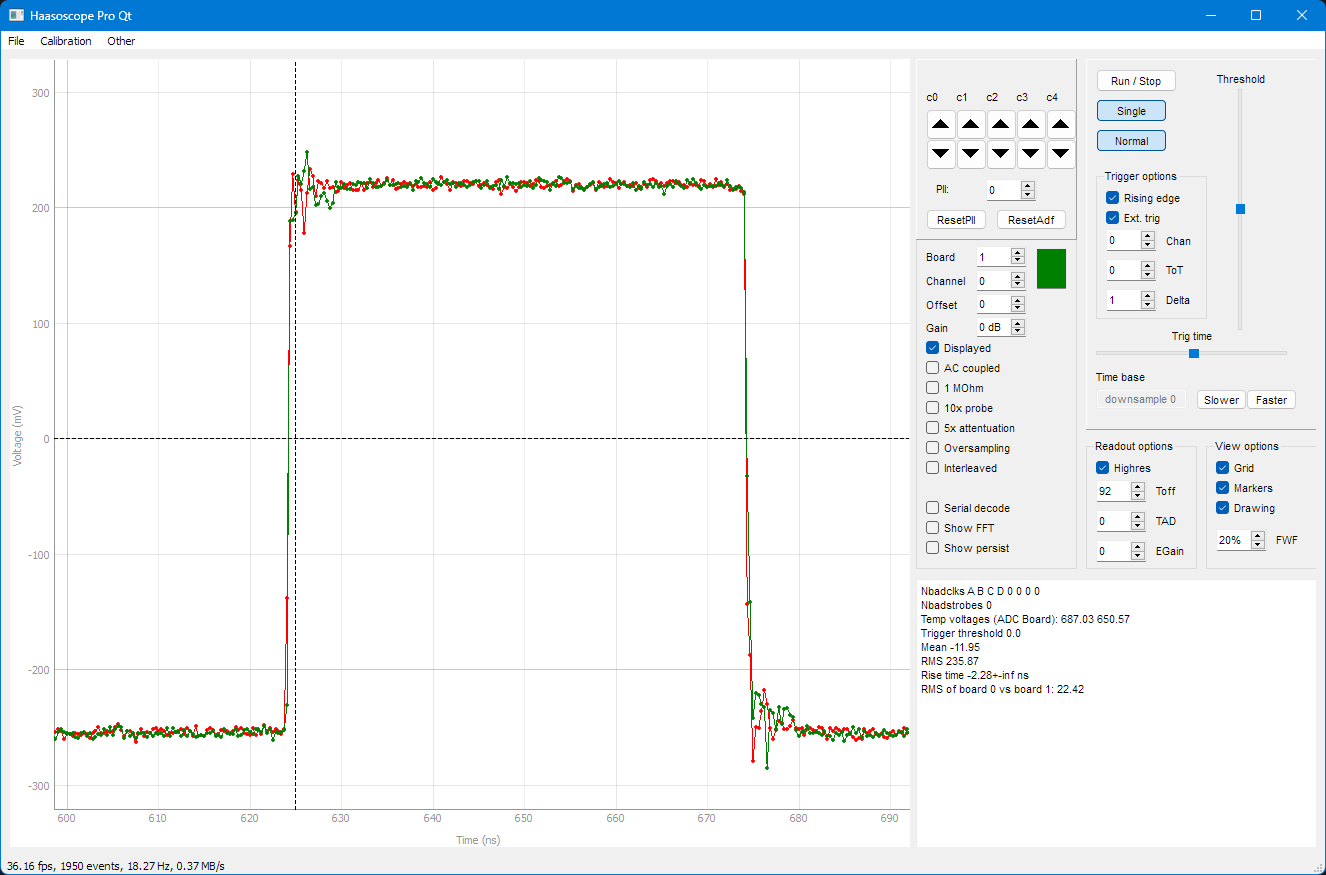
I am sticking with that for now. But before interleaving, we have to shift the sample time for the second board by 1/2 a sample period, which is just 0.5 * 1/3.2GHz = 156.25 ps. Fortunately, our fantastic ADC allows us to shift (delay) the sample time digitally via SPI commands, up to 289 ps, with a resolution of 19 fs!
We're now ready to interleave the samples from the two boards, in software, which gives these results with 6.4 GS/s:
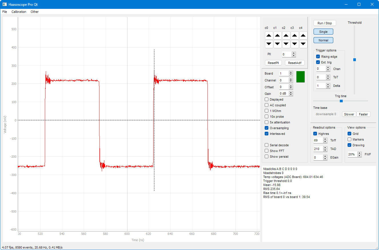
That's a lot of samples on a 10 MHz square wave, and very sharp rising edges. Here's a zoom in of one of those edges:
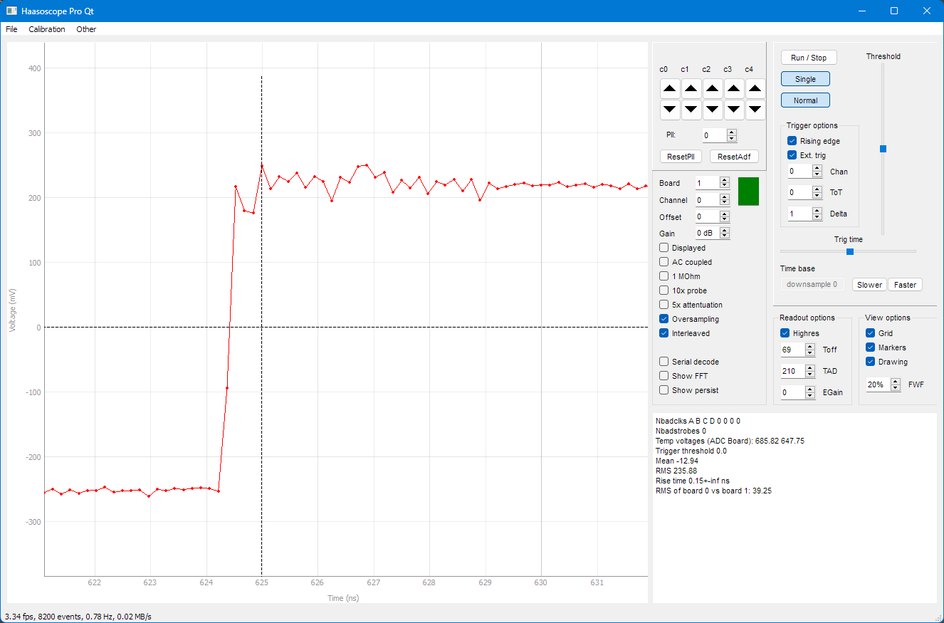
There is still a small amount of high frequency loss on the rising edge, but it's pretty darn good. And that cable/connector impedance mismatch reflection gives a bit of difference between the two boards, leading to the alternating sample "noise" on the plateau after the rising edge. But this performance is still astonishing. We expect at best a risetime of 0.35/2GHz = 175 ps for a bandwidth of 2 GHz, and we are getting at least that. This particular edge, from a pulse generator with a risetime of ~40 ps, had a measured risetime of 150 ps!
 haas
haas
Discussions
Become a Hackaday.io Member
Create an account to leave a comment. Already have an account? Log In.