0%
0%
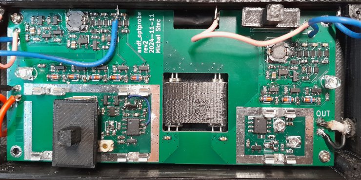
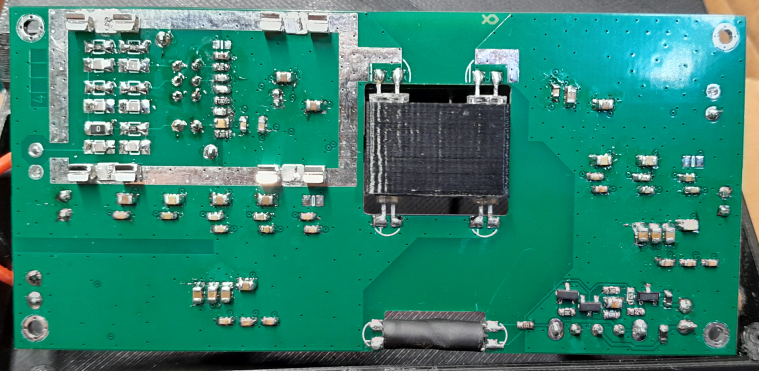
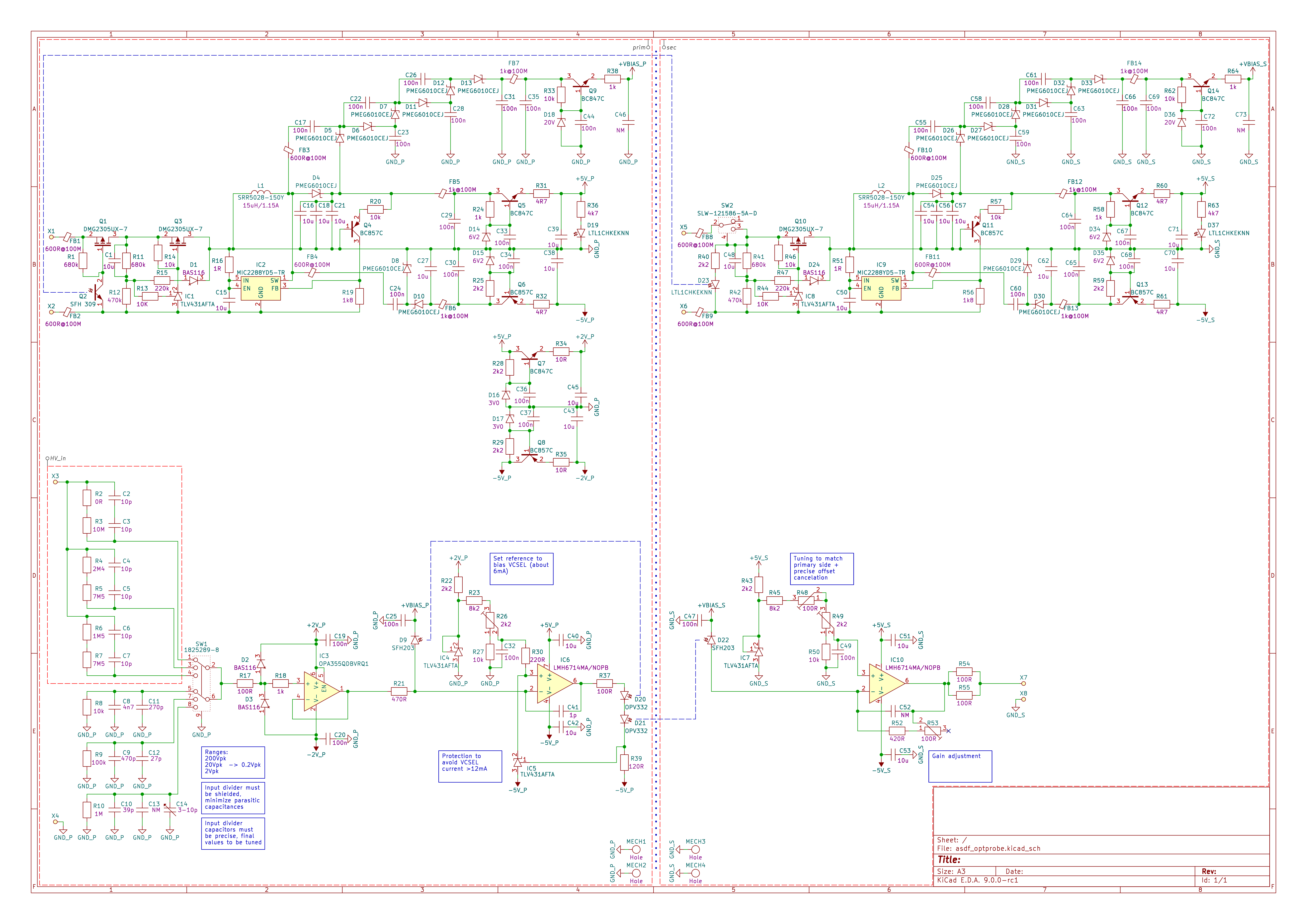
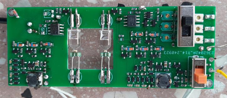
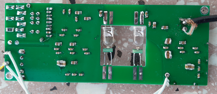
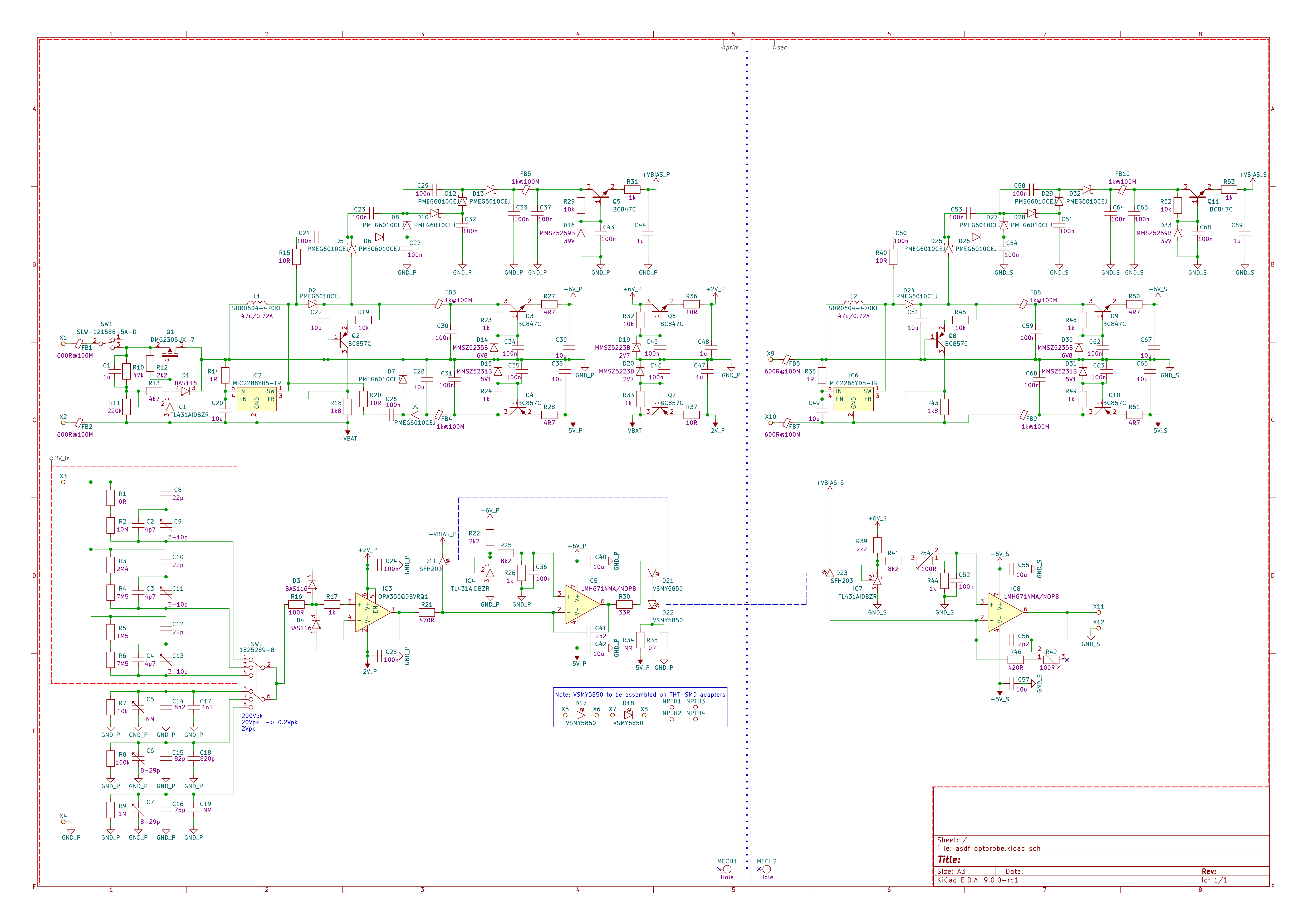
Oscilloscope probe with optical isolation
Isolated probe as an alternative for differential probes
 michal777
Become a Hackaday.io member
Already have an account? Log in.
Just one more thing
To make the experience fit your profile, pick a username and tell us what interests you.
Pick an awesome username
hackaday.io/
Your profile's URL: hackaday.io/username. Max 25 alphanumeric characters.
Pick a few interests
Projects that share your interests
People that share your interests

 Evangelos Petrongonas
 Mitsuru Yamada
 Szoftveres
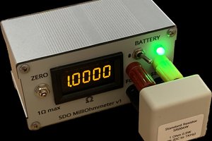
 Kuba Sunderland-Ober