michal777
-
Revision 2
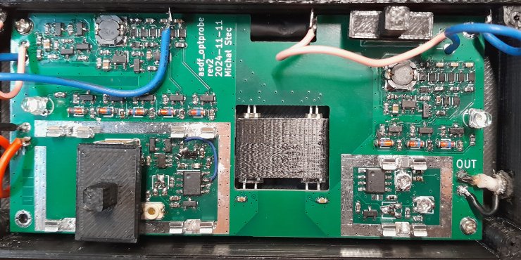
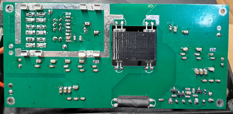
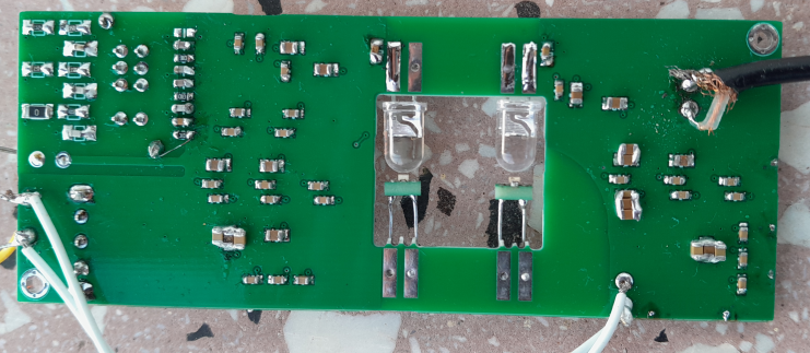
01/01/2025 at 13:00 • 0 commentsRevision 2 is made on 4 layers board and has some shielding to improve noise immunity. Low frequency noise immunity is good but immunity to high frequency noise is still not perfect. Photodiodes were initially not shielded so I had to wrap them in a copper foil to improve immunity. There's still some work to do, to minimize the susceptibility - it's not easy, because the signal is in milivolts range and the device may work near noisy equipment. Possibly a different construction, with very good shielding, including photodiodes, will be needed.
In this revision OPV332 VCSEL emitters were used. Unfortunately they are not perfect - they are usable in small range of power, but with higher power the noise and non-linearity is too bad (the nonlinearity seems "unstable", sawtooth is "wavy" and its shape is easily changed by touching the optical assembly or by small changes of input signal). I don't know reasons of the weird nonlinearity (is it only VCSEL property, or it's more a problem of interaction with photodiode?).
Possibly two versions can be considered in future:
- variant with VSLY3943 LED emitters - linearity is good, bandwidth limited below 10MHz- variant with OPV332 VCSEL emitters - bandwidth over 30MHz, worse linearity and noise
![]()
Issue
Status
Resonance of input wires
A lot of ringing is visible at fast edges. This could be expected and can be reproduced in simulation. Inductance of wires for signal input (hundreds of nH) resonates with input capacitors (about 5pF).
Add 470R resistor in series with input to prevent resonance of the wires with the input capacitance. This 470R is small enough to not cut usable bandwidth.
Bias of TLV431 for laser overload protection
The TLV431 connected directly to the non‑inverting input of the op‑amp changed operating point so that it doesn’t match the secondary side op‑amp.
The TLV431 should have cathode pulled up to positive voltage and be connected through diode to the non‑inverting input of the op‑amp (the diode is not conducting during normal operation).
Voltage drop on photodiode bias
There’s a noticeable voltage drop on a 1k resistor at the output of power supply bias output.
Change the resistor to 100R.
(maybe consider replacing with ferrite, also test if larger filtering capacitor is needed).
No clean turn-off when battery is low
Slow falling edge at the output of the MOSFET doesn’t turn off TLV431 immediately, also battery voltage increases when MOSFET turns off
To be done: try tuning, maybe add more transistors, detect falling edge, further complicate the design
Distortion at some voltage level
Weird distortions observed when OPV331 laser diode was used. Decreasing photodiode current (by decreasing laser current or blocking some light) makes the distortions lower (it also lowers noise).
Maybe two versions are to be considered:
- OPV331 – high speed, worse linearity, bias optimized to lower distortions and noise (low photodiode current, low input amplitude)
- VSLY3943 (alternatively VSMY5850 +external lens*) – low speed, high linearity, larger overshoot because of delay in feedback loop (compensating capacitor can be selected to decrease overshoot or increase bandwidth)
- VSLY3943 – R27=1k6, R39=0R, R37=100R, C41=2p2 (To be done: optimize R37, R39, maybe R21**)
- OPV331 – R27=?, R39=120R, R37=100R, C41=NA (To be done: optimize R27, test different R21, maybe change input divider or range)
* VSMY5850 has lower wavelength (should be good for response time) but nominal response time is lower, it’s SMD and external lens may be needed, possibly slightly better (more tests needed…)
** If emitter is slow, R21 could be increased (slower detector might be not an issue) – tested change from 470R to 1k2 – this made over/under-shoot worse (3%→5%) so it’s still tradeoff.
EM susceptibility
to be investigated...
Part of the problem may be catching the noise in the output coaxial cable (consider output amplifier, consider differential output signal transmission, consider a better coaxial cable although the used one is not bad, possibly unshielded parts which connects to PCB must be as small as possible).
To be done: find out if the noise is caught more in the primary or secondary part of the circuit, check if it gets in through the unshielded photodiode, check if improvements of shielding can help.
- Photodiode seems very susceptible, shield added
Square is not quite square
Distortions of square wave observed – it’s partially caused by not ideal input divider (compensation to be tuned, parasitics unavoidable), also it was distorted when OPV331 with too high light power was used.
- tune input divider on the prototype (will not be final as long as 5% capacitors are used)
- see comments about linearity
-
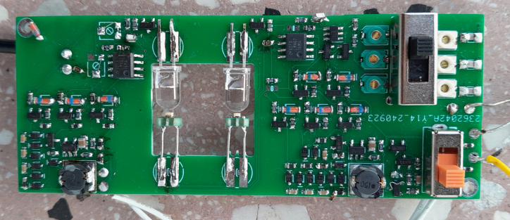
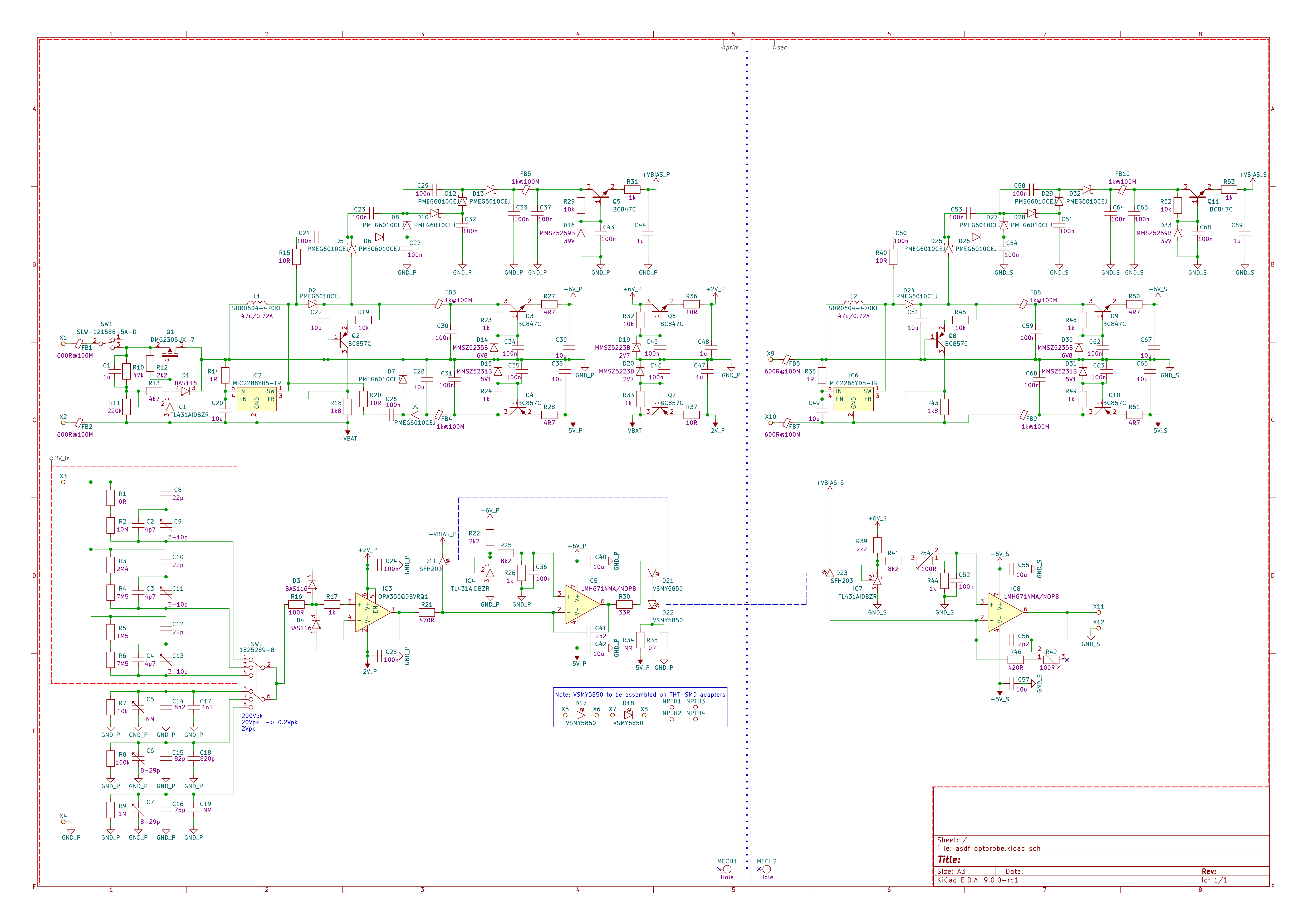
Revision 1
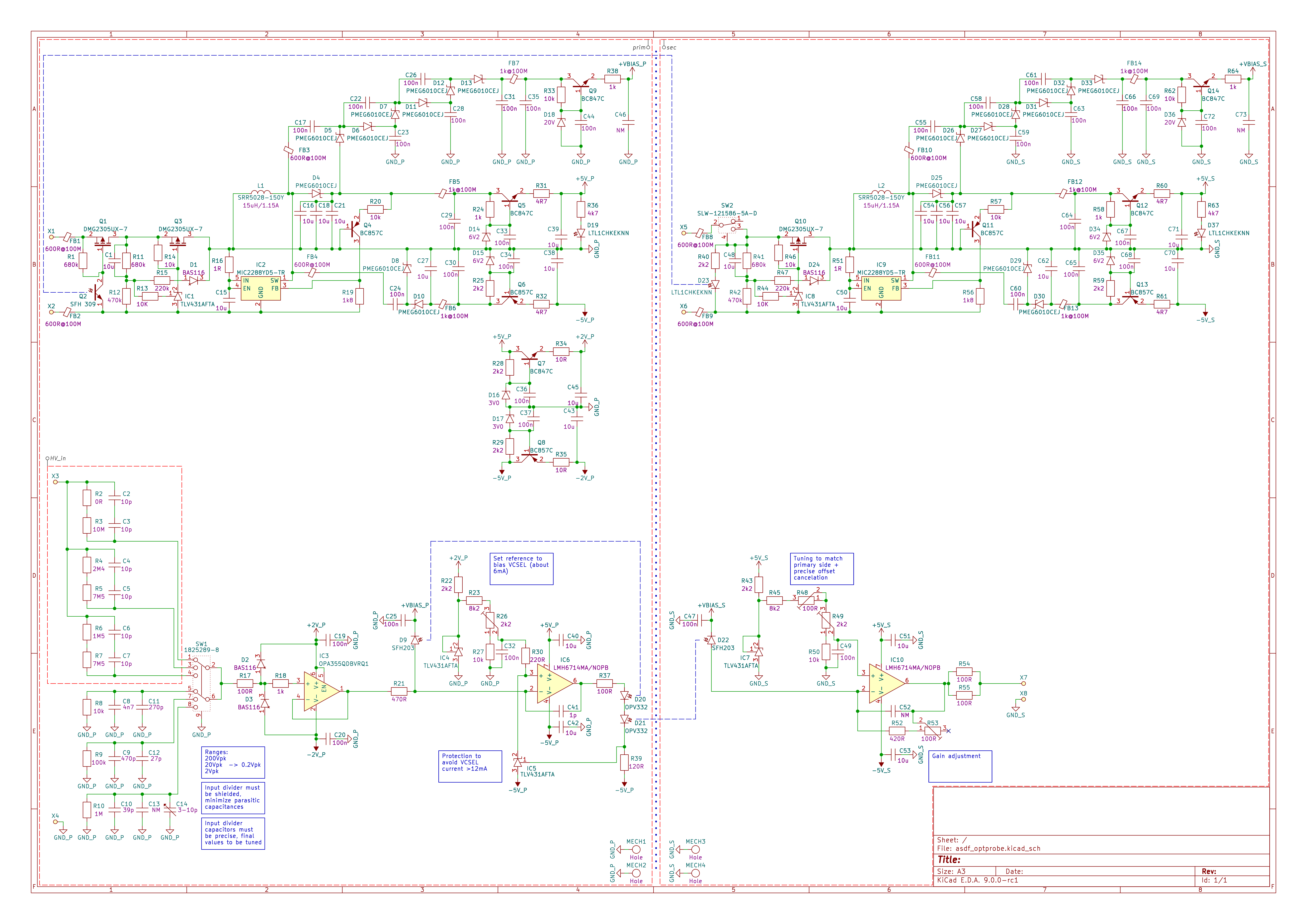
01/01/2025 at 12:27 • 0 commentsThe primary side consists of: power supply, input signal divider (1/10, 1/100, 1/1000), low input capacitance buffer and operational amplifier that drives IR emitters. Feedback of the amplifier includes additional IR emitter and photodiode (the same as on the secondary side) - it's needed for linearization of characteristics of the emitter and detector.
The secondary side consists of: power supply and amplifier that converts photodiode current to the output voltage.
If emitters and detectors have similar characteristics (preferably they are paired), then voltage on R21 and (R42+R46) should be identical (good linearity).
The main problems with the first revision was susceptibility to electromagnetic disturbances: switching noise from internal converters and external SMPSs, also picking up low frequency noise by input voltage divider. Also there were some issues with power supplies or other design issues.
Initially, the infrared emitter was LED, then I started testing VCSEL. VCSEL provided more power at lower current and it was much faster (about 40MHz achieved with VCSEL, with LED it was only about 10MHz). The used VCSEL could be easily overloaded so some active protection was needed in next revision.
![]()
Issue
Status
Can’t turn on.
Under-voltage battery protection issue. Q1 doesn’t turn on after closing the switch. It can turn on if C1 is increased from 1u to 10u. R13 can be increased too.
C1 and resistances are increased. Larger time constant is needed because it takes time to start the boost converter.
Power not delivered at low battery voltage.
Under-voltage battery protection issue. Q1 doesn’t fully turn on if input voltage is low (about 3.4V). Voltage is too low for TL431 so it’s unable to properly bias gate of Q1.
TL431 (Vref=2.495V) replaced by TLV431AFTA (Vref=1.24V). The same reference will be used in other places of the circuit. New resistors values for TLV431AFTA were selected.
Unstable step-up converter.
As datasheet suggests, low inductance and high output capacitance is good for stability. L1 and L2 15uH, C2 and C51 3x10uF works OK.
Tested with #A920CY-150M=P3 (15uH) and output capacitors 3x10u works well. A sililar SRR5028-150Ycan be used instead. The used inductors are magnetically shielded to minimize noise.
Noisy power supply.
Resistors were added at inputs of charge pumps (R15, R20, R40) but they are not enough. Replacing then with ferrite beads helps (1k@100MHz used but it’s maybe too much).
Added ferrite beads at inputs of charge pumps 600R@100MHz.
No signal - saturation.
Incorrect bias for the used emitter+photodiode (VSMY5850 and SFH203). R26 and R44 had to be much lower because VSMY5850 can’t cause that much current through SFH203.
VSMY5850 won’t be used, bias should be designed for IR emitter OPV332. Potentiometers were added to make it adjustable (OPV332+SFH203 may be not very repeatable). Tests shown that 0.7V at “+” input is good for range and linearity (so about 1.5mA through photodiode should flow at 0V input) – voltage divider was adjusted.
Could be faster.
Emitter VSMY5850 and photodiode SFH203 were good up to about 10MHz, C41 was required to avoid ringing. OPV332 (VCSEL) instead of VSMY5850 (LED) works better:
- higher signal (0.4Vpp at output),
- wider bandwidth (probably 30MHz),
- lower current - less heating, so better thermal stability expected (10mA is max, now limited to 5mA).
- THT package (not SMD-THT adapter required)
Higher cost but it’s worth the money.
R30 is changed from 33R to 220R. C41 not placed.
VSMY5850 was changed to OPV332. Cathode must be connected to -5V (not GND) to ensure voltage sufficient for bias (considering op-amp output range and max voltage drop at OPV332). Op-amp output resistor is 220R. A current limiting circuit was added to protect OPV332 from too high current.
Noise susceptibility.
Shielding was not used and it’s clearly essential for acceptable dynamic range. To avoid 50Hz hum and triangle wave from my fluorescent lamp (tens of kHz) it was essential to add shield (copper box) on input signal divider (especially the lower range). Higher frequency noise gets to the signal path through the nets at photodiodes cathodes.
Layout redesigned to add possibility of using shielding boxes. A 4-layer board used and sensitive nets placed inside, between ground planes. D3/D4 input protection diodes are connected to +/-2V which are now better filtered (both 2V regulators are now connected to +/-5V regulators outputs). Photodiodes pads are smaller (leads should be cut short to limit size of “antenna”). Shielding of diodes not planned for now.
Input divider not meeting 200V requirement.
Variable capacitors in upper part of the divider must be avoided or changed to higher voltage.
Simplified. The parts should be precise, not tunable (value of low side capacitors may need to be adjusted one time on a prototype, then compensation should rely on repeatability).
Too high bias voltage of photodiodes.
The photodiodes work with high bias voltage but it’s not recommended (see datasheet). Change bias of diodes.
The diodes are slower at 20V (it’s not clear when and why new absolute maximum limit 20V appeared in SFH203 datasheet). BPV10 at 40V seems not better. The charge pump needs less stages for 20V bias but they are left for now (only zener diode was changed) as maybe a different diode with higher bias and faster response can be still found.
How to power the primary side?
The plan was to use 5V from oscilloscope USB but this is impossible in the current design – signal ground would be at +5V potential.
DON’T use USB in oscilloscope – it’s unclear if USB and signal ground could be safely shorted (after redesign), in general it’s unsafe to connect such DIY things to oscilloscope.
Battery power is used not only for isolated but also for grounded side. It simplifies design and EMC. Primary side will be turned on with help of optocoupler (to avoid two separate on/off switches).
Wrong zener for -5V_S.
D31 value too high – 5.1V makes no sense if input is 5V. It was changed to lower voltage.
New zeners calculated after other changes.
Possible reflections in output coaxial line.
Output will be connected to the oscilloscope through transmission line so reflections may be an issue.
A 50R resistor added at the output of the op-amp. It’s also essential for stability.
Shortcomings.
Diode bias decoupling C44, C69 were 100n, not 1u – maybe enough.
R42, R54 potentiometers were not mounted, but they will be needed (I couldn’t get precise gain and offset) unless paired parts and mechanical tuning will be used (they won’t).
Photodiodes bias decoupling 100n + additional placeholders. Potentiometers – add place for coarse adjustments of IR emitters bias.
Poorly designed.
No calculations, simulations, documentation.
Battery UVLO partially tested and simulated. Boost converter adjusted considering recommendations from datasheet. Calculated zener diodes for +/-5V regulators. Partially simulated OPV332 over-current limit.
Not everything done.
Oscilloscope probe with optical isolation
Isolated probe as an alternative for differential probes