 michal777
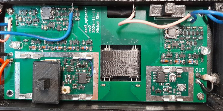
Revision 2 is made on 4 layers board and has some shielding to improve noise immunity. Low frequency noise immunity is good but immunity to high frequency noise is still not perfect. Photodiodes were initially not shielded so I had to wrap them in a copper foil to improve immunity. There's still some work to do, to minimize the susceptibility - it's not easy, because the signal is in milivolts range and the device may work near noisy equipment. Possibly a different construction, with very good shielding, including photodiodes, will be needed.
In this revision OPV332 VCSEL emitters were used. Unfortunately they are not perfect - they are usable in small range of power, but with higher power the noise and non-linearity is too bad (the nonlinearity seems "unstable", sawtooth is "wavy" and its shape is easily changed by touching the optical assembly or by small changes of input signal). I don't know reasons of the weird nonlinearity (is it only VCSEL property, or it's more a problem of interaction with photodiode?).
Possibly two versions can be considered in future:
- variant with VSLY3943 LED emitters - linearity is good, bandwidth limited below 10MHz
- variant with OPV332 VCSEL emitters - bandwidth over 30MHz, worse linearity and noise
Issue |
Status |
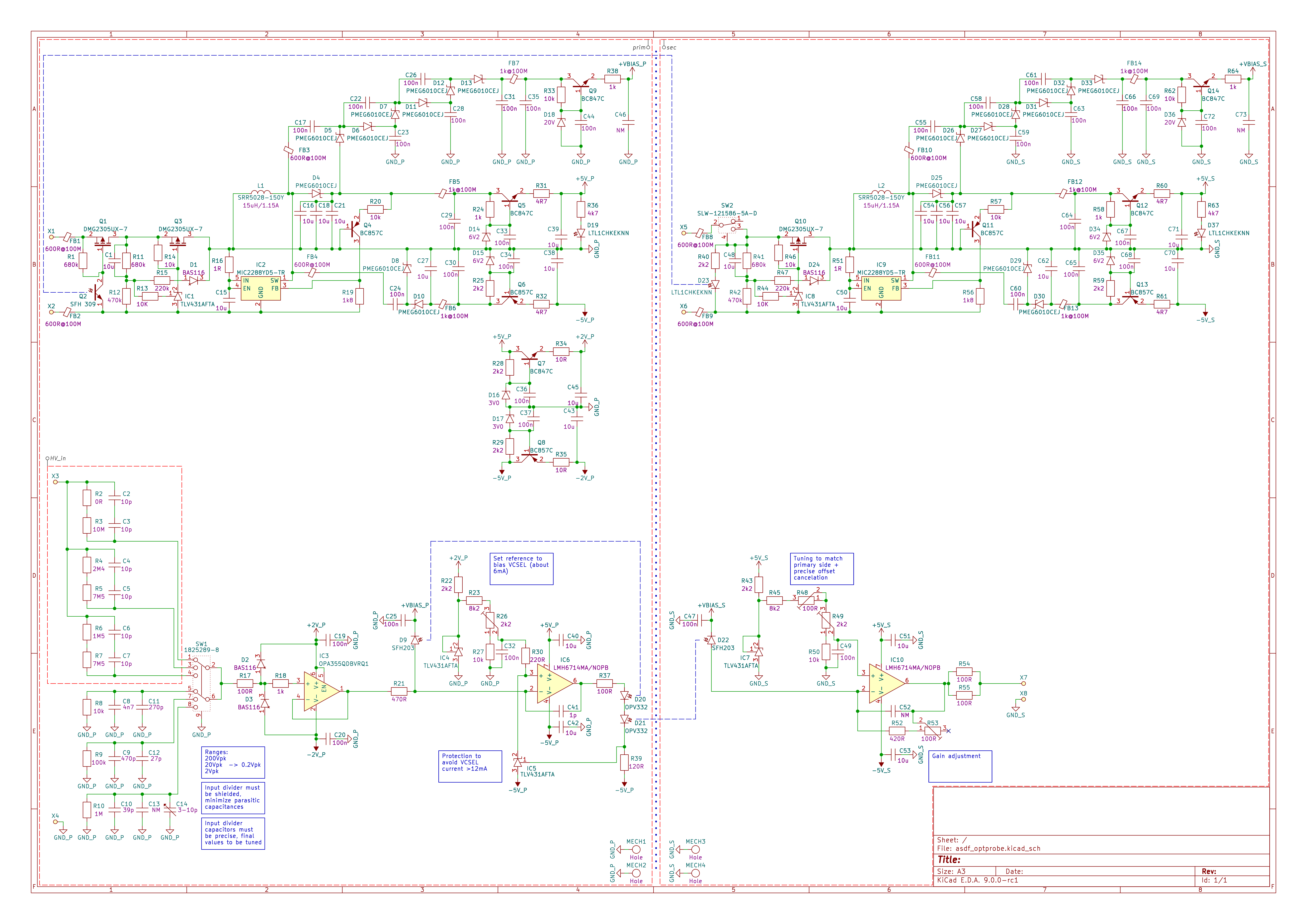
Resonance of input wires A lot of ringing is visible at fast edges. This could be expected and can be reproduced in simulation. Inductance of wires for signal input (hundreds of nH) resonates with input capacitors (about 5pF). |
Add 470R resistor in series with input to prevent resonance of the wires with the input capacitance. This 470R is small enough to not cut usable bandwidth. |
Bias of TLV431 for laser overload protection The TLV431 connected directly to the non‑inverting input of the op‑amp changed operating point so that it doesn’t match the secondary side op‑amp. |
The TLV431 should have cathode pulled up to positive voltage and be connected through diode to the non‑inverting input of the op‑amp (the diode is not conducting during normal operation). |
Voltage drop on photodiode bias There’s a noticeable voltage drop on a 1k resistor at the output of power supply bias output. |
Change the resistor to 100R. (maybe consider replacing with ferrite, also test if larger filtering capacitor is needed). |
No clean turn-off when battery is low Slow falling edge at the output of the MOSFET doesn’t turn off TLV431 immediately, also battery voltage increases when MOSFET turns off |
To be done: try tuning, maybe add more transistors, detect falling edge, further complicate the design |
Distortion at some voltage level Weird distortions observed when OPV331 laser diode was used. Decreasing photodiode current (by decreasing laser current or blocking some light) makes the distortions lower (it also lowers noise). |
Maybe two versions are to be considered: - OPV331 – high speed, worse linearity, bias optimized to lower distortions and noise (low photodiode current, low input amplitude) - VSLY3943 (alternatively VSMY5850 +external lens*) – low speed, high linearity, larger overshoot because of delay in feedback loop (compensating capacitor can be selected to decrease overshoot or increase bandwidth) - VSLY3943 – R27=1k6, R39=0R, R37=100R, C41=2p2 (To be done: optimize R37, R39, maybe R21**) - OPV331 – R27=?, R39=120R, R37=100R, C41=NA (To be done: optimize R27, test different R21, maybe change input divider or range) * VSMY5850 has lower wavelength (should be good for response time) but nominal response time is lower, it’s SMD and external lens may be needed, possibly slightly better (more tests needed…) ** If emitter is slow, R21 could be increased (slower detector might be not an issue) – tested change from 470R to 1k2 – this made over/under-shoot worse (3%→5%) so it’s still tradeoff. |
EM susceptibility to be investigated... |
Part of the problem may be catching the noise in the output coaxial cable (consider output amplifier, consider differential output signal transmission, consider a better coaxial cable although the used one is not bad, possibly unshielded parts which connects to PCB must be as small as possible). To be done: find out if the noise is caught more in the primary or secondary part of the circuit, check if it gets in through the unshielded photodiode, check if improvements of shielding can help. - Photodiode seems very susceptible, shield added |
Square is not quite square Distortions of square wave observed – it’s partially caused by not ideal input divider (compensation to be tuned, parasitics unavoidable), also it was distorted when OPV331 with too high light power was used. |
- tune input divider on the prototype (will not be final as long as 5% capacitors are used) - see comments about linearity |
Discussions
Become a Hackaday.io Member
Create an account to leave a comment. Already have an account? Log In.