BeanZee Z80 development board
This project started out as the Z80 breadboard computer and the schematic is largely the same. I wanted to move to something more robust and permanent before going on to a more complex design, but I also realised that by building a development board (a little like the Arduino UNO) this could provide a reliable base for experimenting with further designs.
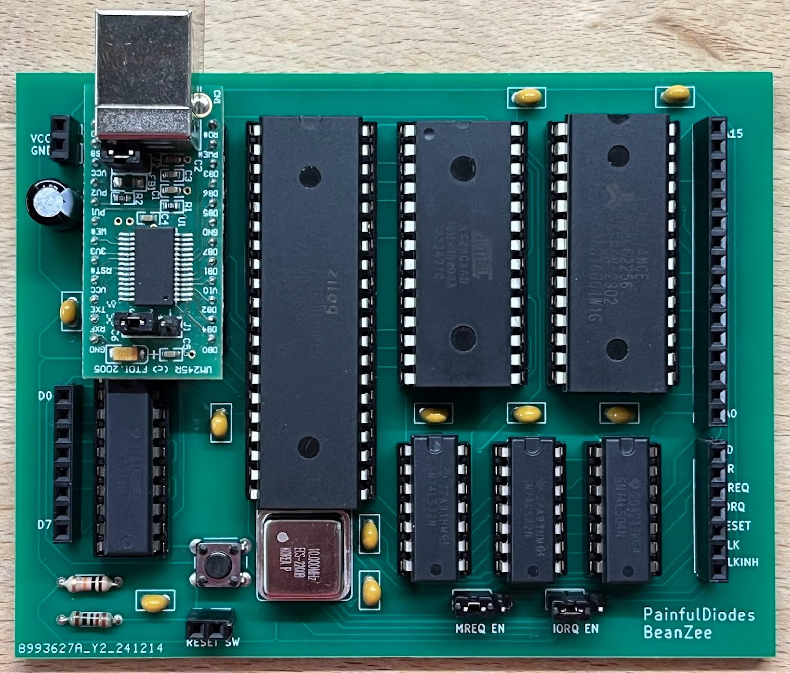
The board has a 10MHz Z80 CPU, a clock module, 32k RAM, 32k EEPROM - which needs to be programmed externally, a simple reset circuit and an FTDI UM245R USB module.
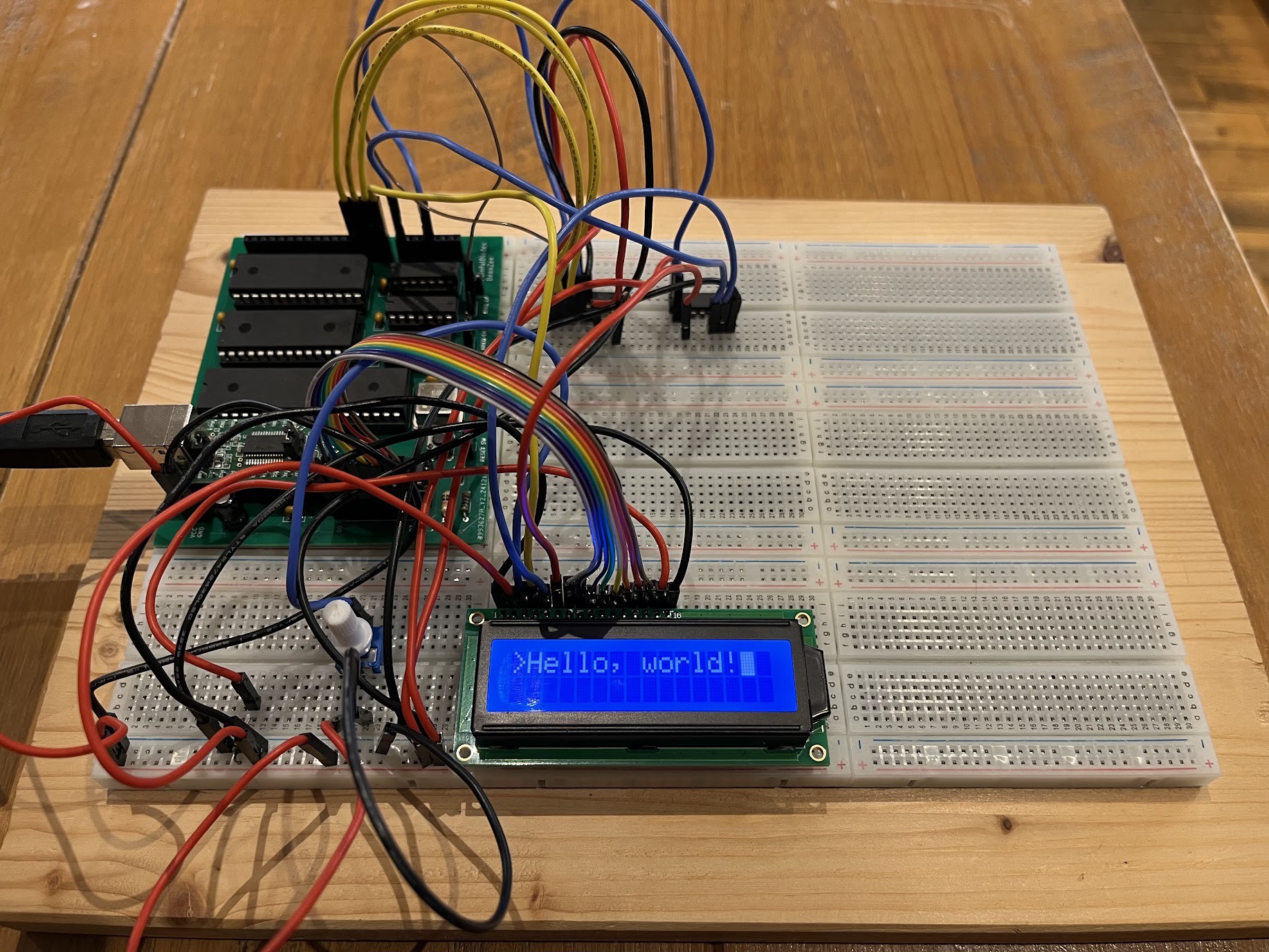
Marvin is a very simple monitor program, through which it is possible to load, inspect / modify (in hex) and execute a program on the BeanZee via the USB interface and a terminal emulator.
High level design
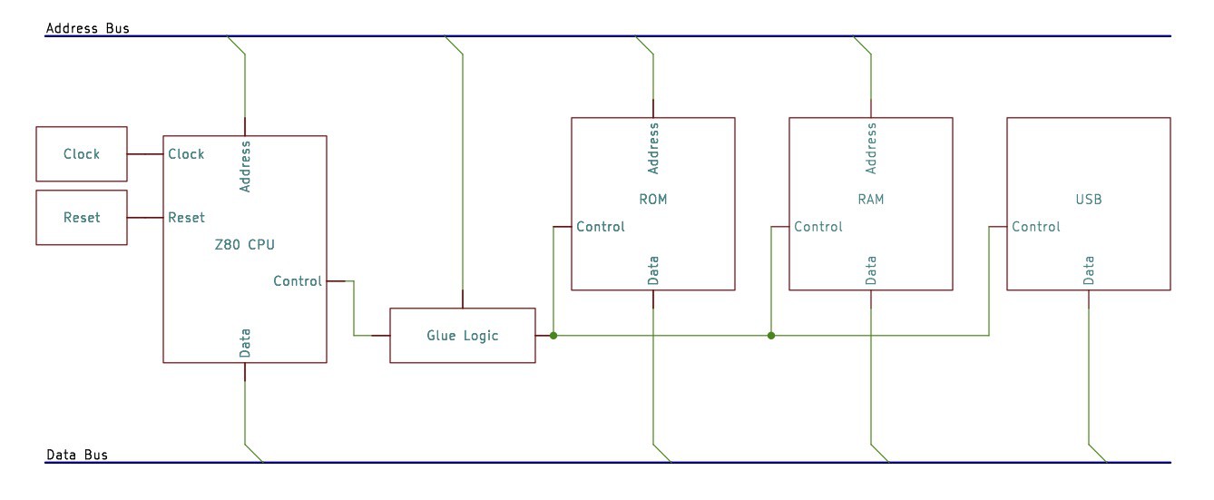
For a minimal but usable design I have used an FTDI USB development board. This choice was guided by Keith's Hackaday project.
I want to have some software that can run from power-up, which will be preprogrammed onto EEPROM. This will be loaded with a monitor program, and interpreters which will allow other programs to be loaded into RAM and executed from a computer connected via USB.
Schematics
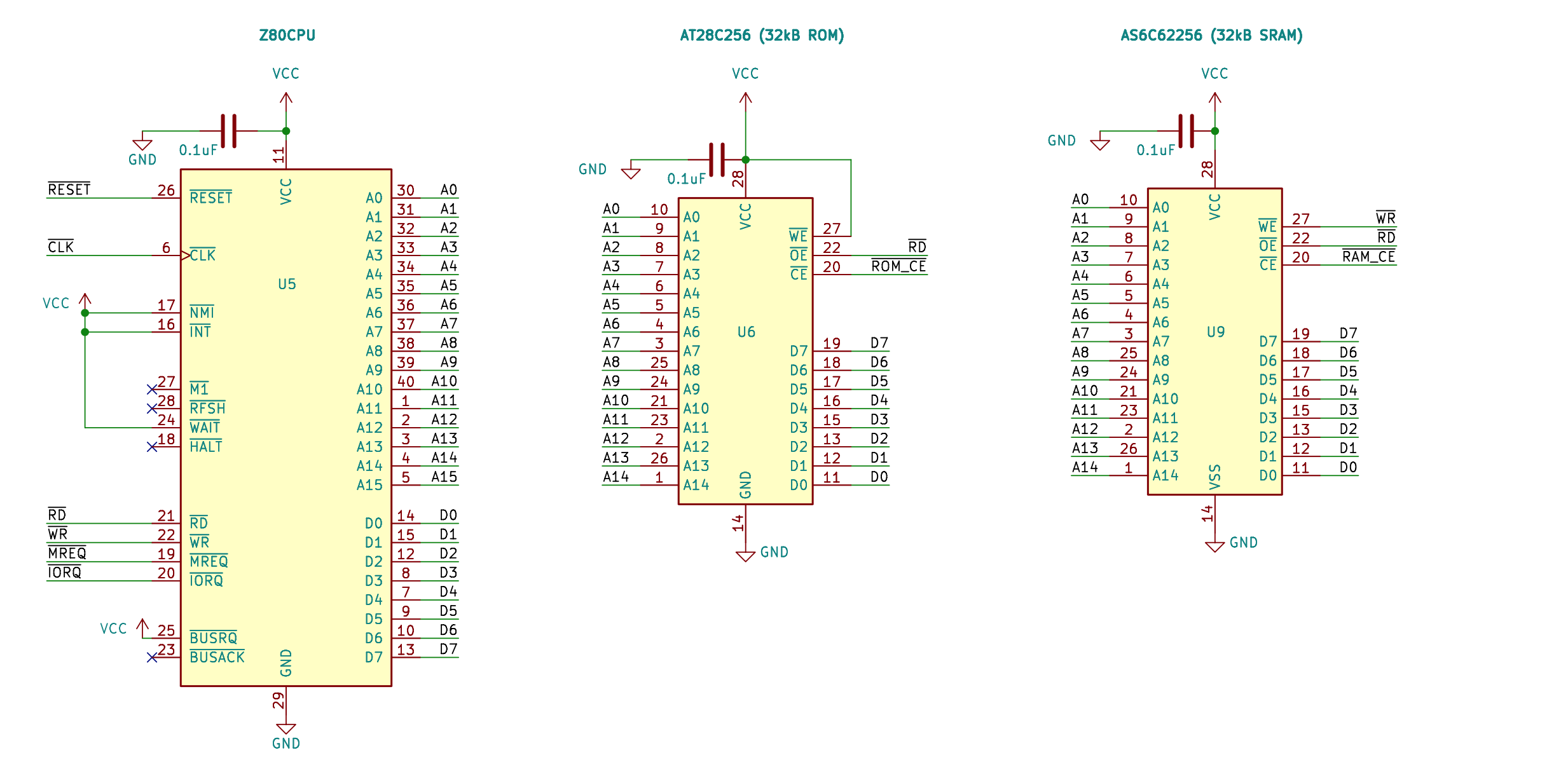
At the heart of the board is the Z80 CPU. Those control inputs which for our purposes need to remain inactive (/NMI, /INT, /WAIT, /BUSRQ) are wired high. We'll be ignoring some of the control outputs like /BUSAK, which are left disconnected.
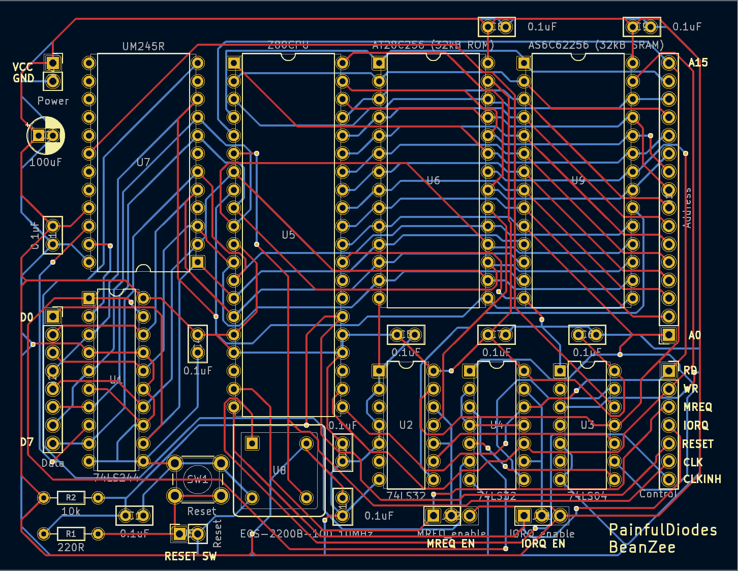
For memory I have an AS6C62256, 32K x 8 SRAM and an AT28C256 32K x 8 EEPROM. This makes for a very usable small system, but the simple memory map also keeps the address decoding really simple - device selection based on A15.
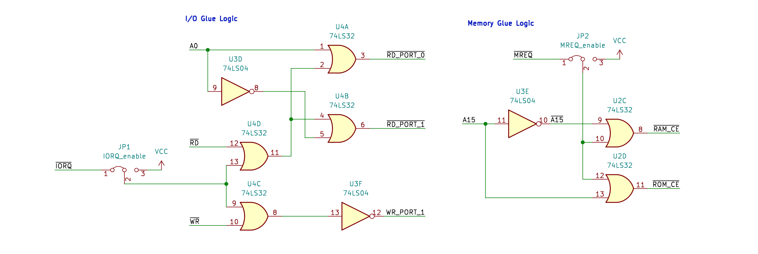
I/O decoding is minimal. When operating as a self-contained board, we only have to consider the USB module - from which the CPU reads and writes data on one port (1) and reads status on another port (0). To keep the logic as simple as possible, in effect: port 0 will be read for any even-numbered port, port 1 will be read for any odd-numbered port, and port 1 will be written to for any port number.
However, if we want to connect external I/O, this logic will be insufficient. JP1 allows us to accommodate this.
With JP1 connecting pins 1 and 2, the board will operate as above - with the USB.
With JP1 connecting pins 2 and 3, the USB will be disabled, and external I/O devices may be connected.
If no jumper is present, an external circuit may be connected to pin 2. Additional external logic may be used for example to enable the USB for a specific port range.
JP2 provides the same options for adding external memory.
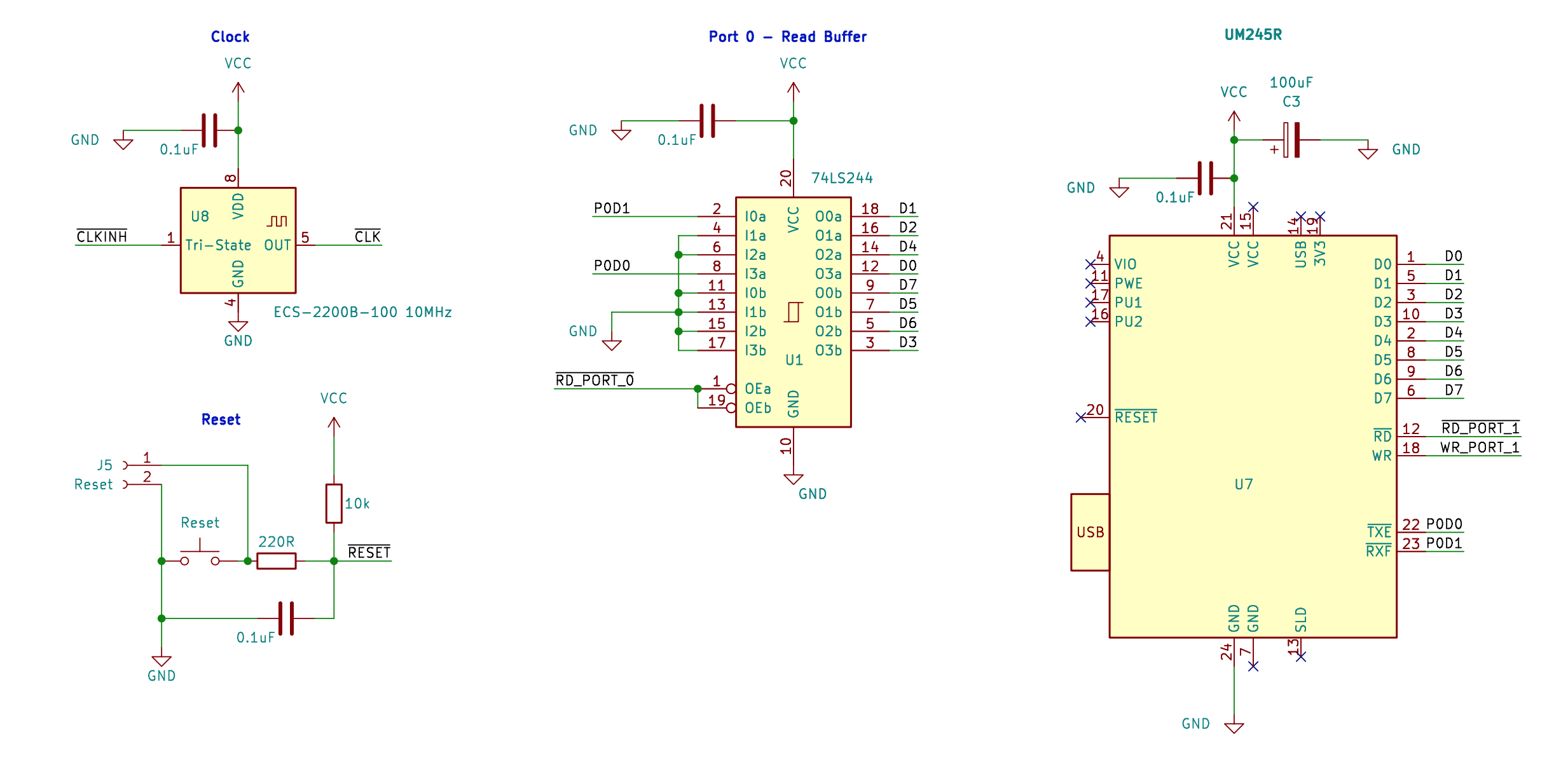
The clock module has an input to enable / disable operation. This has been made accessible as /CLKINH on a socket alongside CLK - see the connectors diagram, below.
If /CLKINH is left disconnected the on-board clock will operate normally. If /CLKINH is taken low the clock will stop, and the clock module output will go into a high impedance state. This means that an external clock generator could be connected to CLK.
The USB module has /TXE (transmit ready) and /RXF (buffer has data) outputs. To make these accessible to the CPU, I have connected them to the data bus on D0 and D1 via a tri-state buffer. The glue logic then opens the buffer allowing these signals onto the data bus when requested.
Note that the board can be powered via the USB interface.

As a development board, there are a number of connectors for experimentation. Address and data bus connectors, /RD, /WR, /IORQ and /MREQ allow the CPU to address external memory and ports.

PCB
I designed a double-sided PCB in KiCAD, and had this produced at JLCPCB.
 Stephen Willcock



Nice clean design. I like to port some kind of BASIC onto my CPU projects to demonstrate they can do something, but now that everyone has access to cross assemblers and compilers it make more sense just to have a hex file downloader and let the user load anything they want. I shall be taking that approach in future, especially for CPUs for which I have no BASIC or other demo firmware.