 Stephen Willcock
At one point I had intended widening the ground and power tracks on the PCB, but didn't do it in the end. Having shared the design around for comment, the puny power tracks were called out, and I had a couple of suggestions to upgrade to a 4 layer board. This would allow for generous ground and power planes, and make the layout actually much easier.
Aside from the easier layout, the suggestion was that this arrangement would clean up the power to the chips across the board.
To check this out I tested the board with my 40 year old oscilloscope:
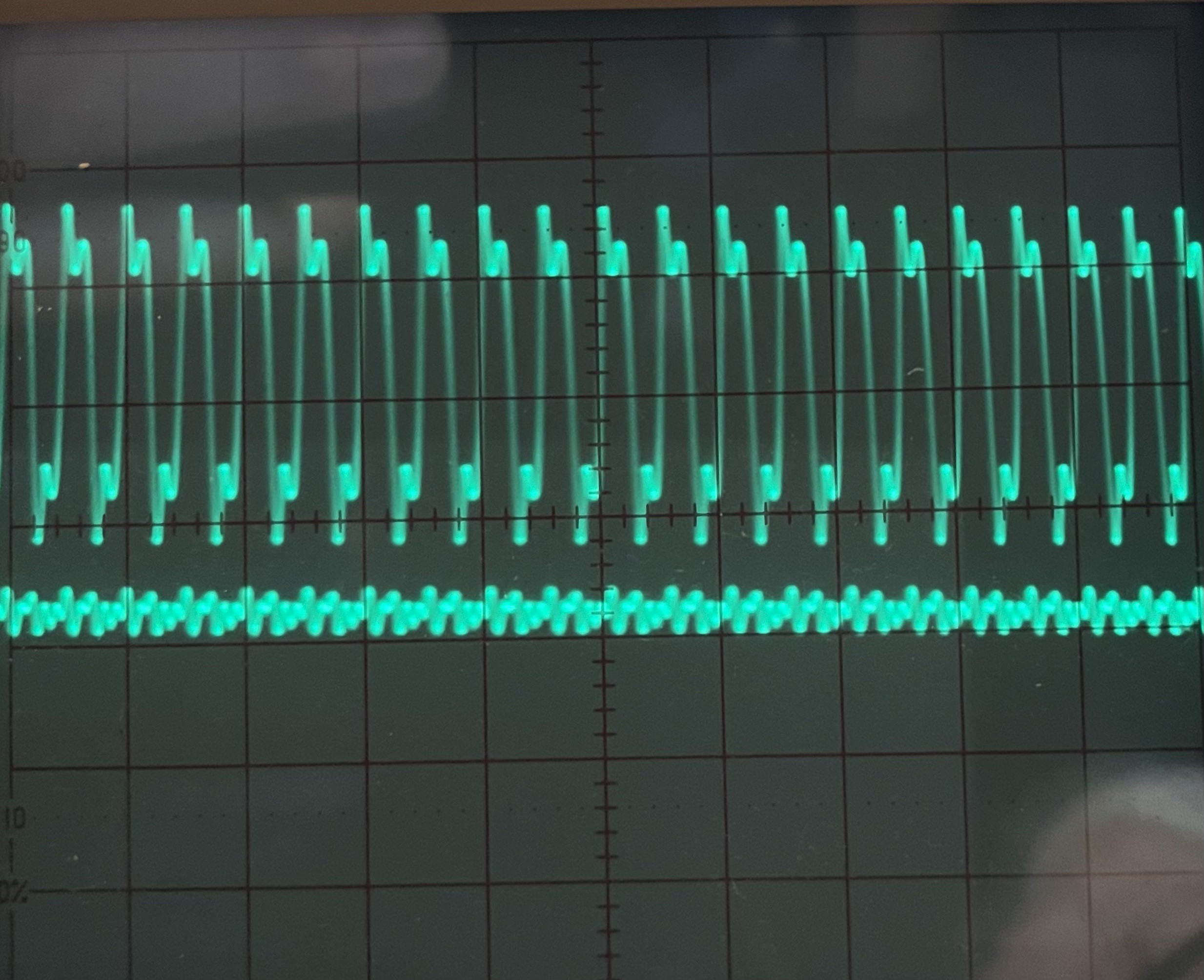
The top trace is the clock, and the lower trace is the +5v measured at the opposite end of the board from where the supply enters the board.
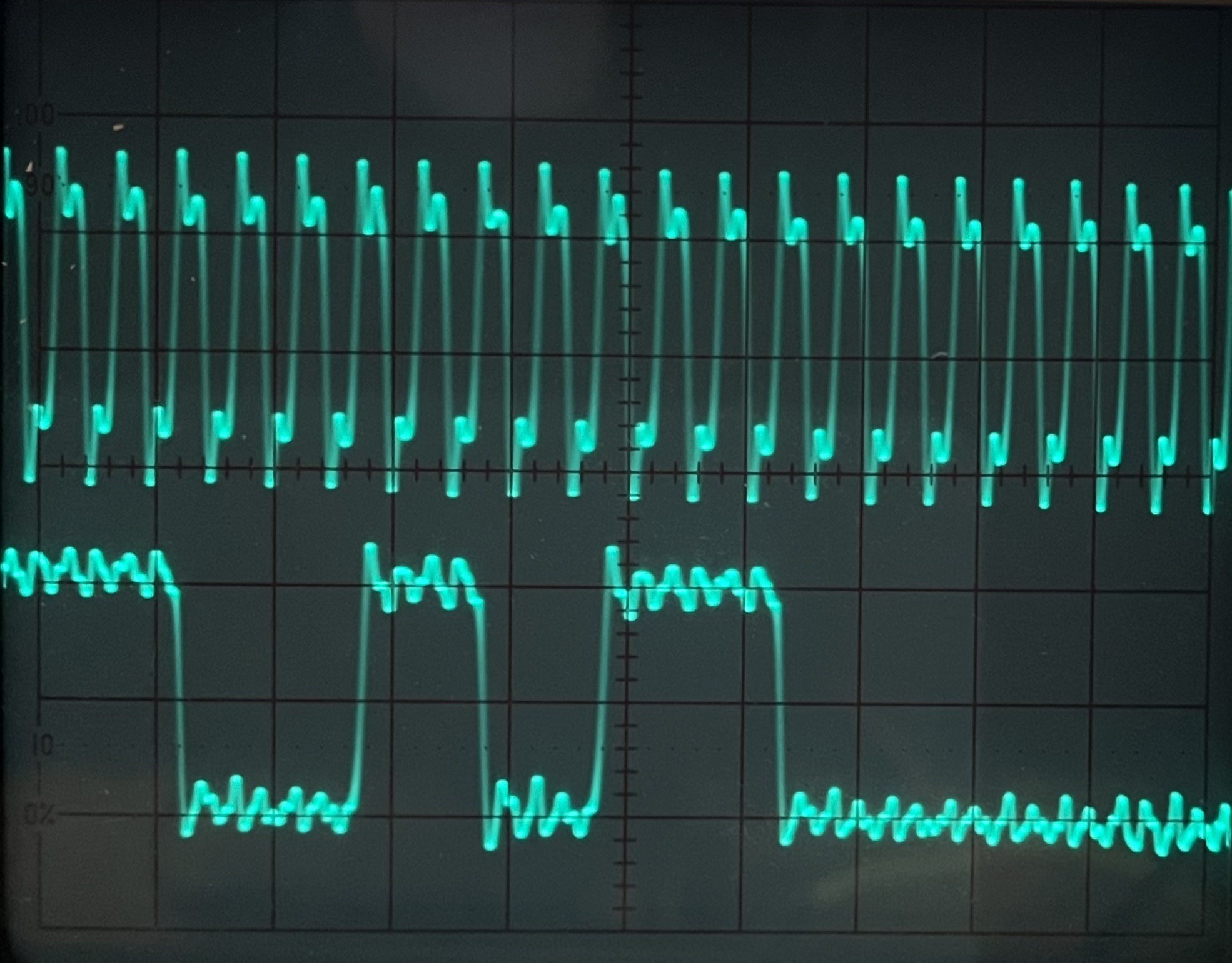
As a matter of interest, I tested one of the address lines (again at the edge of the board). The CPU was running in a loop waiting for input, so the pattern was stable:
Finally for comparison I checked the clock and power on the prototype (matrixboard/wire construction):
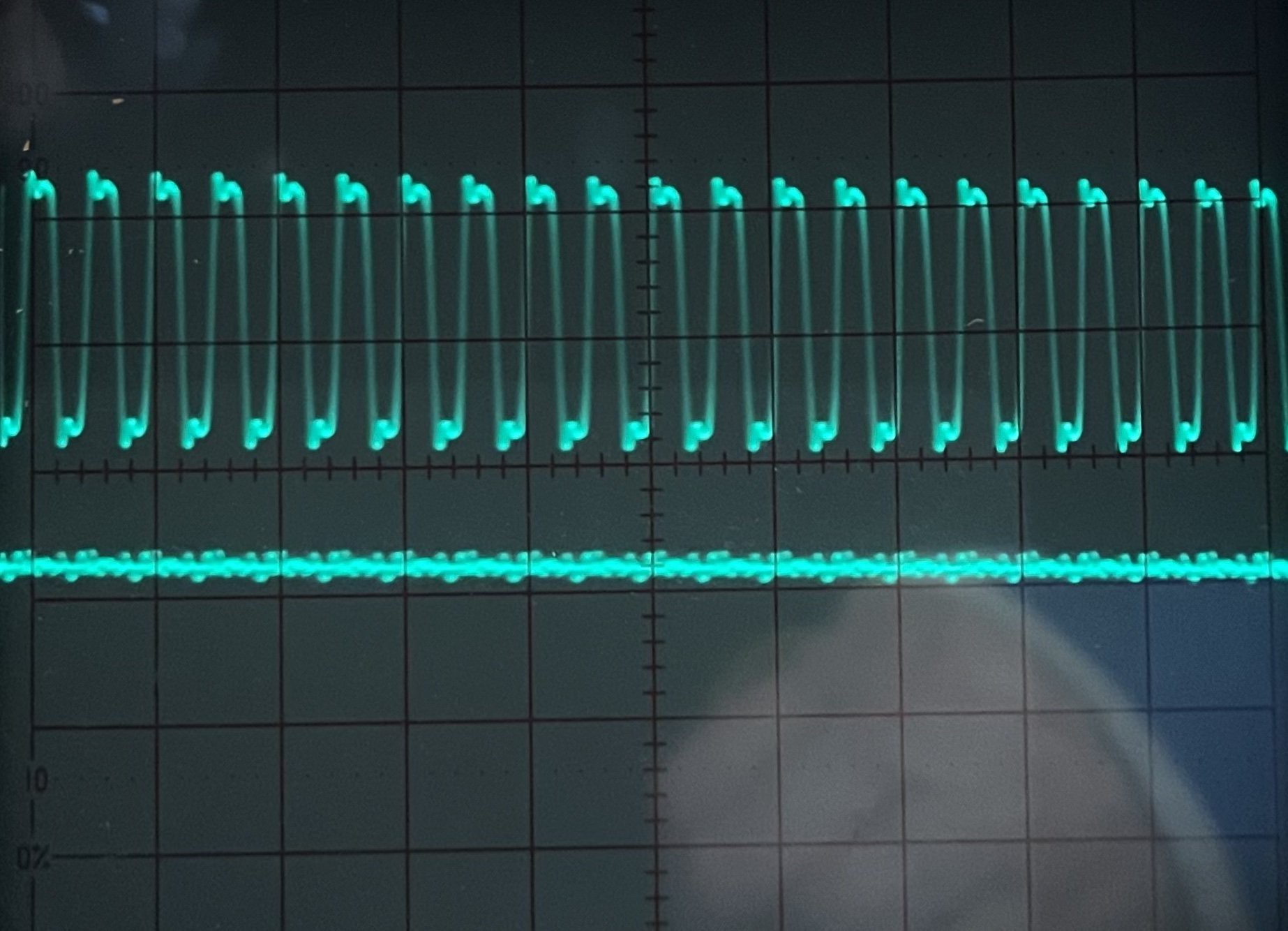
This is a lot cleaner than the PCB.
I plan to rework the PCB into 4 layers, and will do a 3-way comparison then.
Discussions
Become a Hackaday.io Member
Create an account to leave a comment. Already have an account? Log In.