Close
0%
0%

BeanZee

Z80 homebrew development board

Similar projects worth following
A small Z80 homebrew single-board-computer designed for experimentation.

Z80 CPU, 10 MHz clock, a simple reset circuit, 32K ROM, 32K RAM, FTDI UM245R USB module and the necessary glue logic.

Connectors provided for interfacing with the Z80: address, data, read, write, IO request, memory request, clock and reset.

The internal clock may be overridden by an external clock, and the internal memory and USB module may also be disabled via jumpers so that external devices can be used, or additional memory and IO selection logic added.

There is also an accompanying monitor program which can be used to load and execute programs from a host computer.

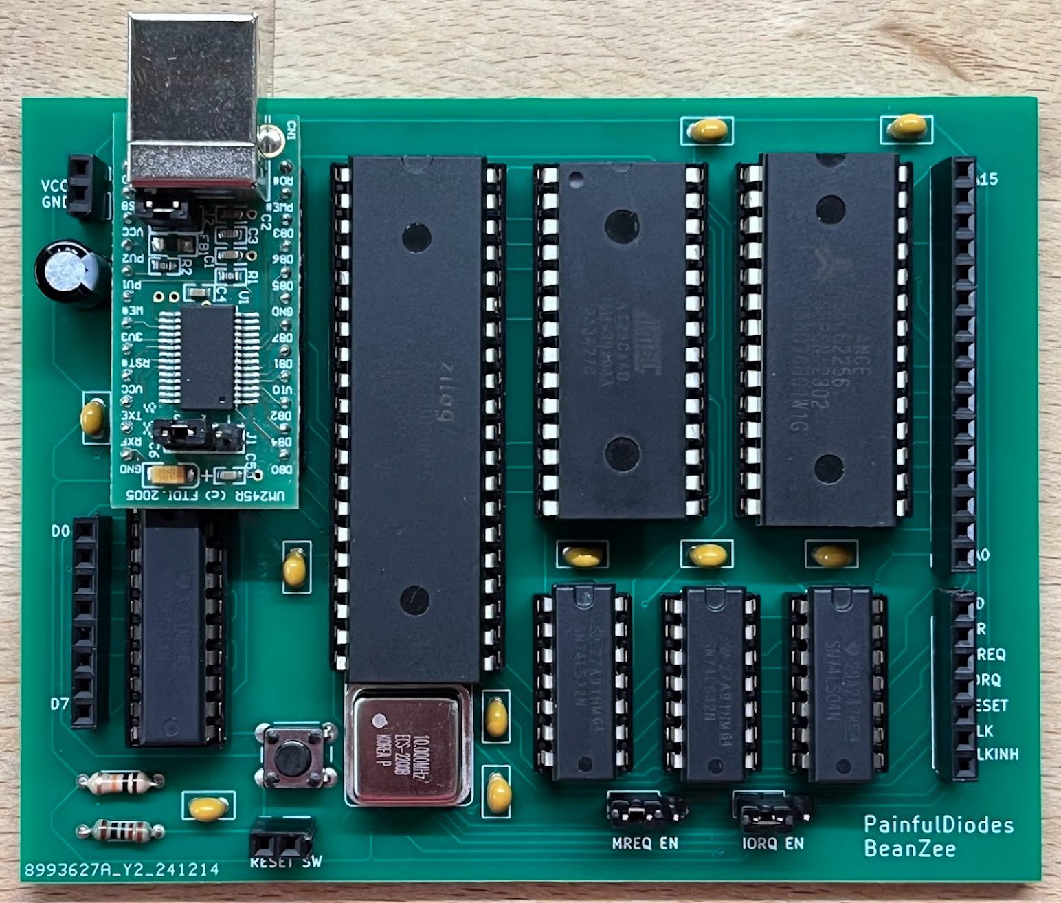
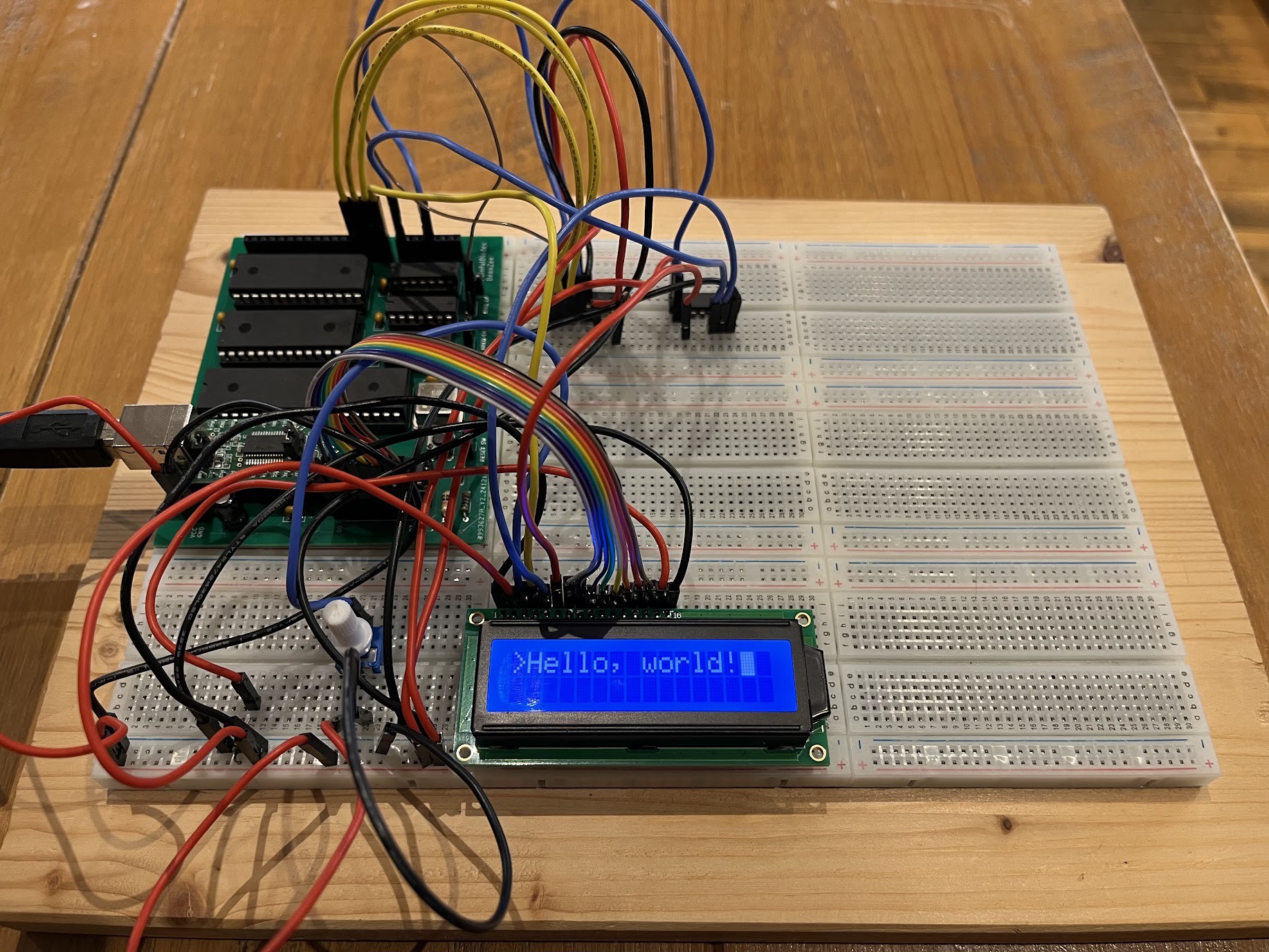
BeanZee Z80 development board

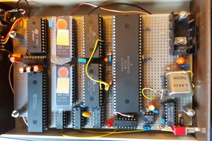
This project started out as the Z80 breadboard computer and the schematic is largely the same. I wanted to move to something more robust and permanent before going on to a more complex design, but I also realised that by building a development board (a little like the Arduino UNO) this could provide a reliable base for experimenting with further designs.

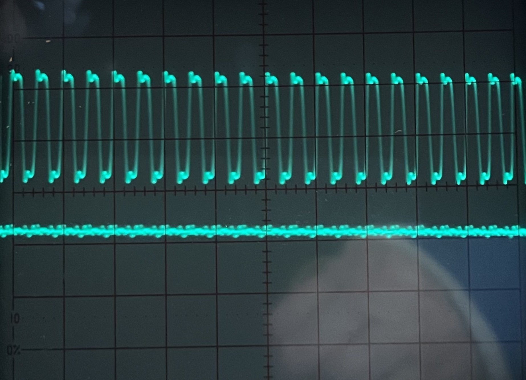
The board has a 10MHz Z80 CPU, a clock module, 32k RAM, 32k EEPROM - which needs to be programmed externally, a simple reset circuit and an FTDI UM245R USB module.

Marvin is a very simple monitor program, through which it is possible to load, inspect / modify (in hex) and execute a program on the BeanZee via the USB interface and a terminal emulator. 

High level design

For a minimal but usable design I have used an FTDI USB development board. This choice was guided by Keith's Hackaday project

I want to have some software that can run from power-up, which will be preprogrammed onto EEPROM. This will be loaded with a monitor program, and interpreters which will allow other programs to be loaded into RAM and executed from a computer connected via USB.

Schematics

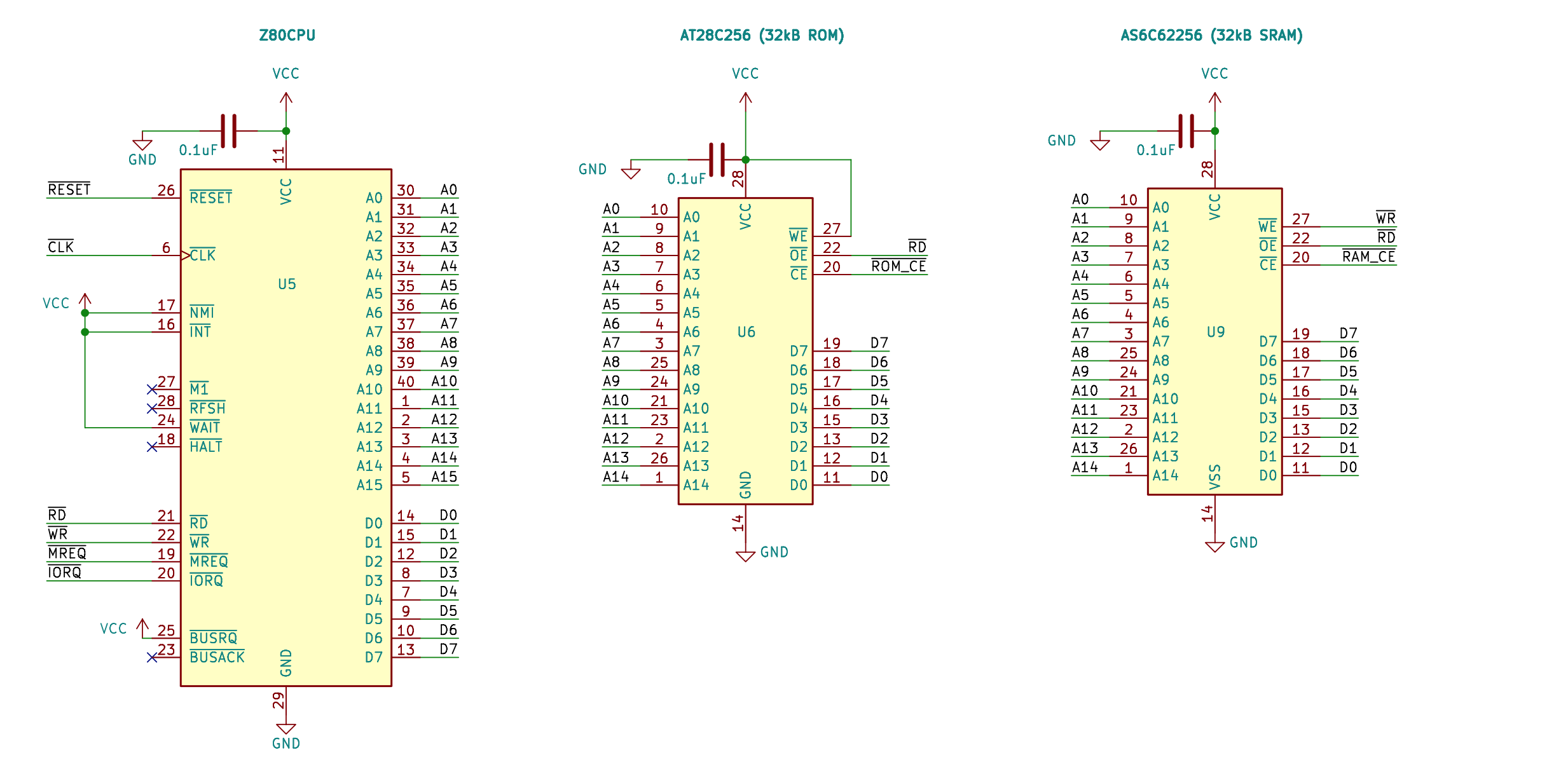
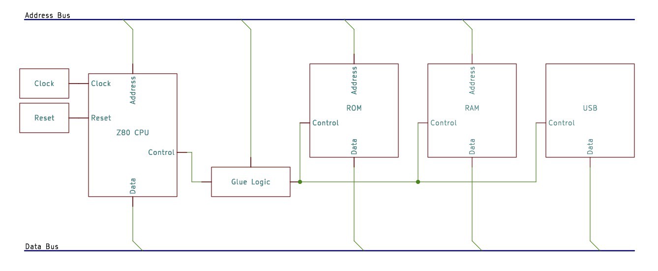
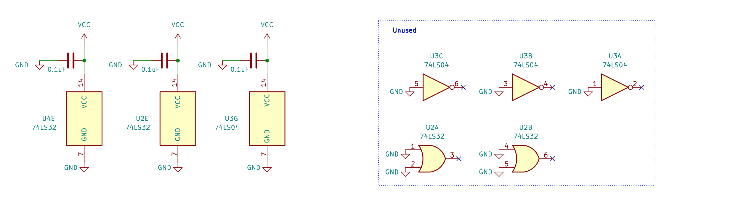
At the heart of the board is the Z80 CPU. Those control inputs which for our purposes need to remain inactive (/NMI, /INT, /WAIT, /BUSRQ) are wired high. We'll be ignoring some of the control outputs like /BUSAK, which are left disconnected.

For memory I have an AS6C62256, 32K x 8 SRAM and an AT28C256 32K x 8 EEPROM. This makes for a very usable small system, but the simple memory map also keeps the address decoding really simple - device selection based on A15.

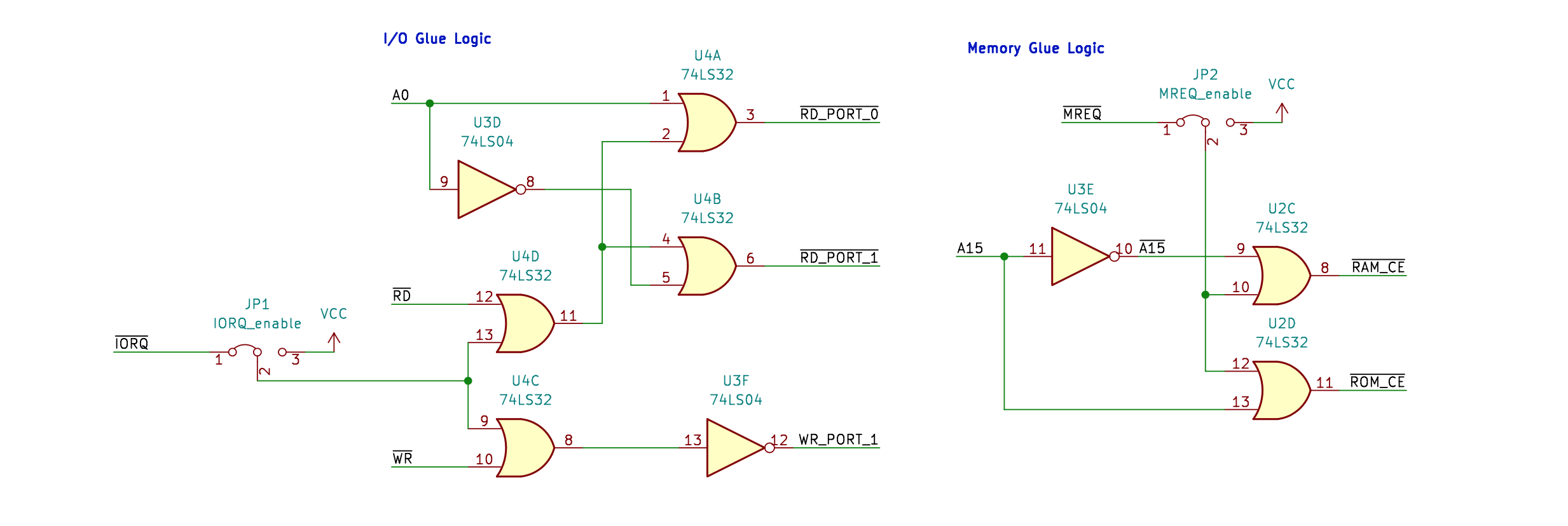
I/O decoding is minimal. When operating as a self-contained board, we only have to consider the USB module - from which the CPU reads and writes data on one port (1) and reads status on another port (0). To keep the logic as simple as possible, in effect: port 0 will be read for any even-numbered port, port 1 will be read for any odd-numbered port, and port 1 will be written to for any port number.

However, if we want to connect external I/O, this logic will be insufficient. JP1 allows us to accommodate this. 

With JP1 connecting pins 1 and 2, the board will operate as above - with the USB.

With JP1 connecting pins 2 and 3, the USB will be disabled, and external I/O devices may be connected.

If no jumper is present, an external circuit may be connected to pin 2. Additional external logic may be used for example to enable the USB for a specific port range.

JP2 provides the same options for adding external memory.

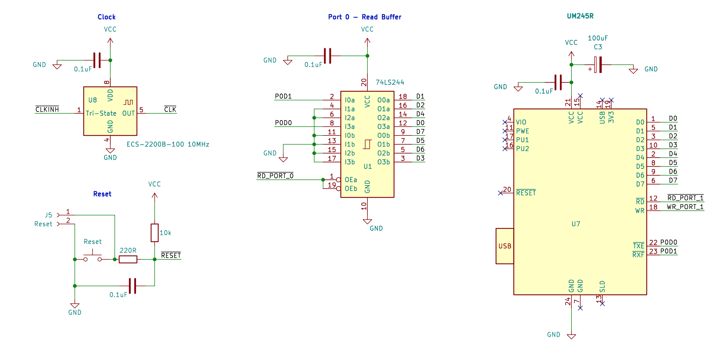
The clock module has an input to enable / disable operation. This has been made  accessible as /CLKINH on a socket alongside CLK - see the connectors diagram, below.

If /CLKINH is left disconnected the on-board clock will operate normally. If /CLKINH is taken low the clock will stop, and the clock module output will go into a high impedance state. This means that an external clock generator could be connected to CLK.

The USB module has /TXE (transmit ready) and  /RXF (buffer has data) outputs. To make these accessible to the CPU, I have connected them to the data bus on D0 and D1 via a tri-state buffer. The glue logic then opens the buffer allowing these signals onto the data bus when requested.

Note that the board can be powered via the USB interface.

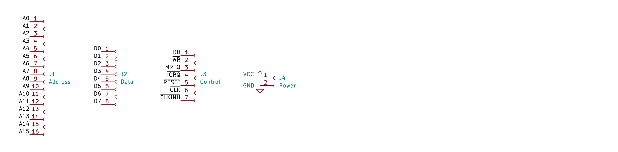
As a development board, there are a number of connectors for experimentation. Address and data bus connectors, /RD, /WR, /IORQ and /MREQ allow the CPU to address external memory and ports.
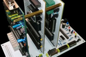
PCB

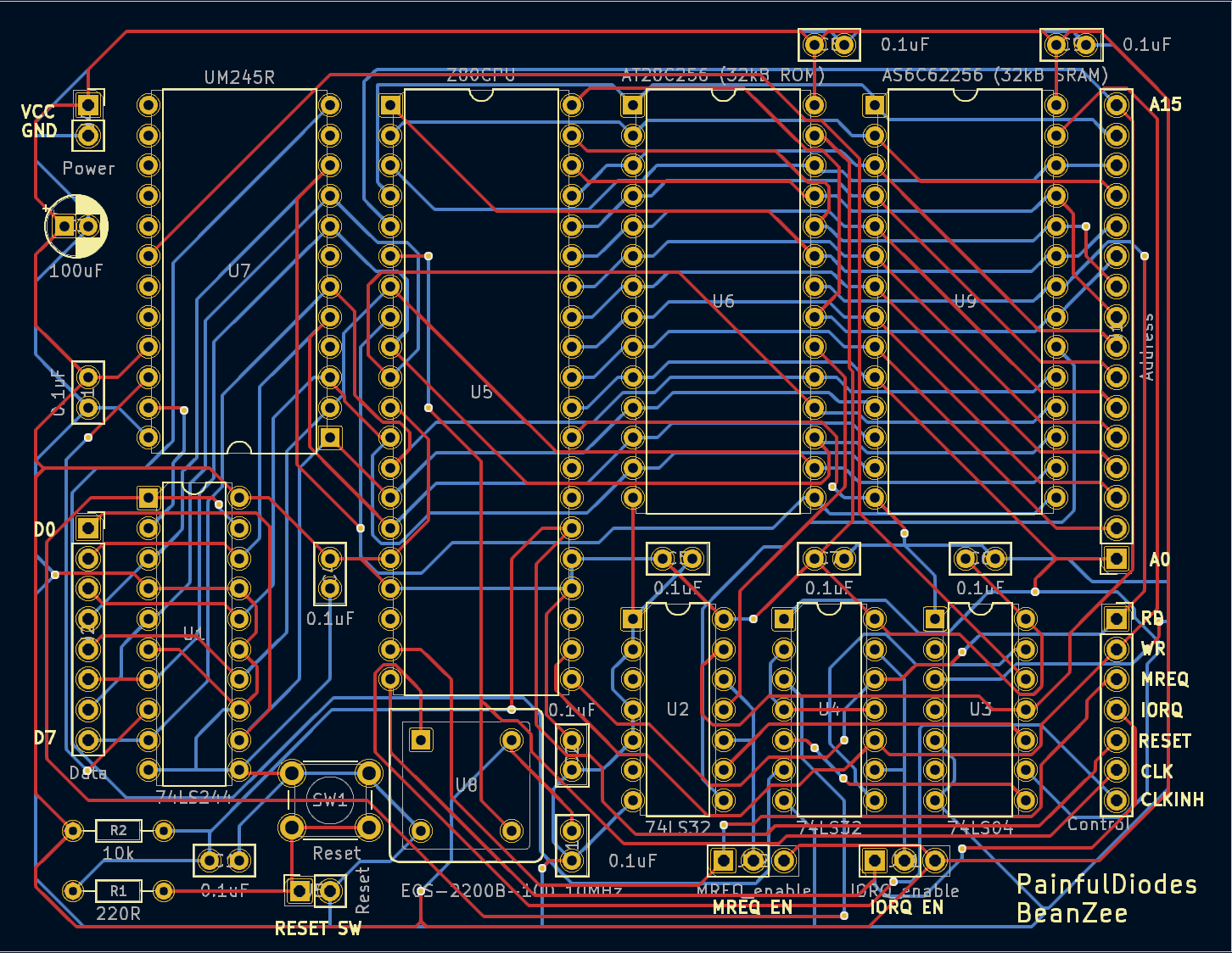
I designed a double-sided PCB in KiCAD, and had this produced at JLCPCB.

gbr.zip

BeanZee Gerber files

Zip Archive - 32.60 kB - 01/15/2025 at 07:55

Download

BeanZee.pdf

BeanZee schematics

Adobe Portable Document Format - 492.99 kB - 01/15/2025 at 07:53

Preview

  • BeanBoard prototype

    Stephen Willcock2 days ago 0 comments

    Assembled the BeanBoard over the weekend. Generally happy - managed to load and run some test programs showing things are working as expected. However there are some significant issues… the buttons and the board are way too large - I thought the larger tactile buttons might be a mistake, and they are. I need to shrink the whole thing, and move the logic underneath the BeanZee piggyback board. The LCD may need to be angled to read easily, but this too may be solved just by making the board smaller. But the biggest problem was that I bungled the switches on the layout. On the schematic I used a generic switch and then later added a specific button footprint. Problem was I should have replaced the switches on the schematic, which would have made the pinouts explicit. As it was, all the switches were shorted. Removing the diodes and patching with links to correct the wiring works, but is a real pain. Lesson learned.

  • Video clip of BeanZee keypad and LCD

    Stephen Willcock5 days ago 0 comments

    Just uploaded a video clip of my breadboard experiment - keypad and LCD display

  • BeanBoard PCB design

    Stephen Willcock03/29/2025 at 14:41 0 comments

    Having proven the LCD display and QWERTY keyboard design on breadboard, this week I designed a PCB in KiCAD and have now sent off an order to JLCPCB. As planned, the BeanZee Z80 homebrew, and an LCD module will plug into this new PCB, forming a small self-contained computer.

    I have some misgivings about the choice of buttons. Originally I was looking at using small tactile buttons, but was worried they would be too fiddly for my large digits.

    I've gone for larger tactile buttons, which has made the PCB quite large (327 mm x 199 mm). Given the size of the PCB, I could switched to Cherry MX keyboard buttons, but these would have pushed the overall price up. I have compromised and stuck with the tactile buttons. We shall see!

    https://github.com/PainfulDiodes/BeanBoard

  • QWERTY... or just Q so far

    Stephen Willcock03/22/2025 at 16:19 0 comments

    Homebrew Z80 QWERTY keyboard prototype going quite nicely... ultimately this is going to be an 8x8 keyboard matrix, but for now I have 4x2. All the glue logic seems to be working as planned.

    https://github.com/PainfulDiodes/BeanBoard

    Echo

  • BeanBoard breadboard

    Stephen Willcock03/20/2025 at 13:12 0 comments

    Started prototyping the BeanBoard keyboard/LCD display on breadboard. Added port address decoding and the LCD display, and succeeded with a Hello World program for the LCD display on the BeanZee board.

    https://github.com/PainfulDiodes/BeanZeeBytes/tree/main/asm_examples/beanboard_helloworld

    https://github.com/PainfulDiodes/BeanBoard

  • BeanZee console game - Snake

    Stephen Willcock03/16/2025 at 13:17 0 comments

    Just added a simple console game to my BeanZee examples repo. This one I originally coded a couple of years ago for a simple Arduino idea - with interaction via a touchscreen. This one is all text via a VT100/ANSI terminal emulator 

  • BeanZeeBytes

    Stephen Willcock03/07/2025 at 16:22 0 comments

    Just added a couple of "hello world" examples for how BeanZee/Marvin Z80 development board should work, in a new repo: https://github.com/PainfulDiodes/BeanZeeBytes

    I think it pulls the project together a bit better. I'll try and get a more interesting example up, but this will be really useful when there's more hardware too.

  • Marvin the Monitor v1

    Stephen Willcock02/27/2025 at 07:42 0 comments

    Finally Marvin, my tiny monitor program, is sufficiently complete to be usable / useful with BeanZee.

    https://github.com/PainfulDiodes/marvin

    With it you can now:

    • Read from memory as hex data
    • Write hex data to memory
    • Load a program from an Intel HEX format file
    • Execute a program from a specific address

    This means you can build a program on your host computer using a cross-assembler or cross-compiler, and so long as you can produce an Intel HEX file you can load and run the program on BeanZee via a terminal emulator.

    The repo includes a couple of really simple test programs.

    I have been using SjASMPlus for assembling Marvin, but this does not include the means to generate Intel HEX output. For this I am using z88dk-appmake. 

    I will be taking another look at z88dk, as this seems to have a comprehensive toolset for Z80 work.

  • LCD output experiment

    Stephen Willcock02/12/2025 at 14:31 0 comments

    I’d like to provide direct inputs and outputs for  BeanZee. I have some ideas around a fairly minimal keyboard matrix for input and for output, having considered several options I’ve decided to use an LCD character display.

    My reentry into hobby electronics in 2020 was via an Arduino starter kit, which conveniently includes an LCD device. On further investigation, this device uses a Hitachi HD44780 LCD controller which was developed in the 1980’s and appears to be the de facto standard for character (as opposed to graphics) LCD drivers. There are many variants, but most seem to adhere to a standard 16 line interface.

    I want to work out how I might hook this up to a Z80, and I am going to get the display working with an Arduino UNO (r3). There is an LCD library for the Arduino which provides a bunch of simplifications for using the device, and the source for this is on GitHub and should help me to understand how to interface and use the device.

    Following the Liquid Crystal Displays (LCD) with Arduino article I very quickly got a hello world output from the device:

    I also wrote a sketch to simulate the behaviour I will be aiming for – reading keystrokes from the USB interface and printing them to the LCD.

    This was actually very useful, as it helped me understand how I will use the available commands in the LCD controller to implement terminal output to the LCD – handling backspace, CR/LF, line wrapping and scrolling.

    Reading the LCD library source code was also useful. Following the flow of outputs it seems that the natural sequencing of the Z80 control and data lines for I/O should also work, subject to the speed/timing being compatible.

    Subsequently I looked to see if there is a RC2014 example of a Hitachi HD44780 LCD, and was pleased to find that there is: https://rc2014.co.uk/modules/lcd-driver-module/

    This page also links to Mike Sutton’s blog post on Connecting an LCD to a Z80 with Two Glue Chips which very helpfully describes in detail timing, including nuances between using /RD rather than /WR to control R/W, so next steps with the Z80 are looking promising.

    Experiment files: https://github.com/PainfulDiodes/experiments/tree/main/arduino-lcd-experiment

  • Noisy BeanZee

    Stephen Willcock02/02/2025 at 17:16 0 comments

    At one point I had intended widening the ground and power tracks on the PCB, but didn't do it in the end. Having shared the design around for comment, the puny power tracks were called out, and I had a couple of suggestions to upgrade to a 4 layer board. This would allow for generous ground and power planes, and make the layout actually much easier.

    Aside from the easier layout, the suggestion was that this arrangement would clean up the power to the chips across the board.

    To check this out I tested the board with my 40 year old oscilloscope:

    The top trace is the clock, and the lower trace is the +5v measured at the opposite end of the board from where the supply enters the board. 

    As a matter of interest, I tested one of the address lines (again at the edge of the board). The CPU was running in a loop waiting for input, so the pattern was stable:

    Finally for comparison I checked the clock and power on the prototype (matrixboard/wire construction):

    This is a lot cleaner than the PCB. 

    I plan to rework the PCB into 4 layers, and will do a 3-way comparison then.

View all 10 project logs

Enjoy this project?

Share

Discussions

Rich text editor

Keith wrote 03/23/2025 at 17:06 point

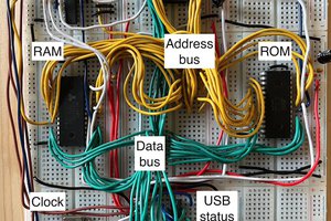
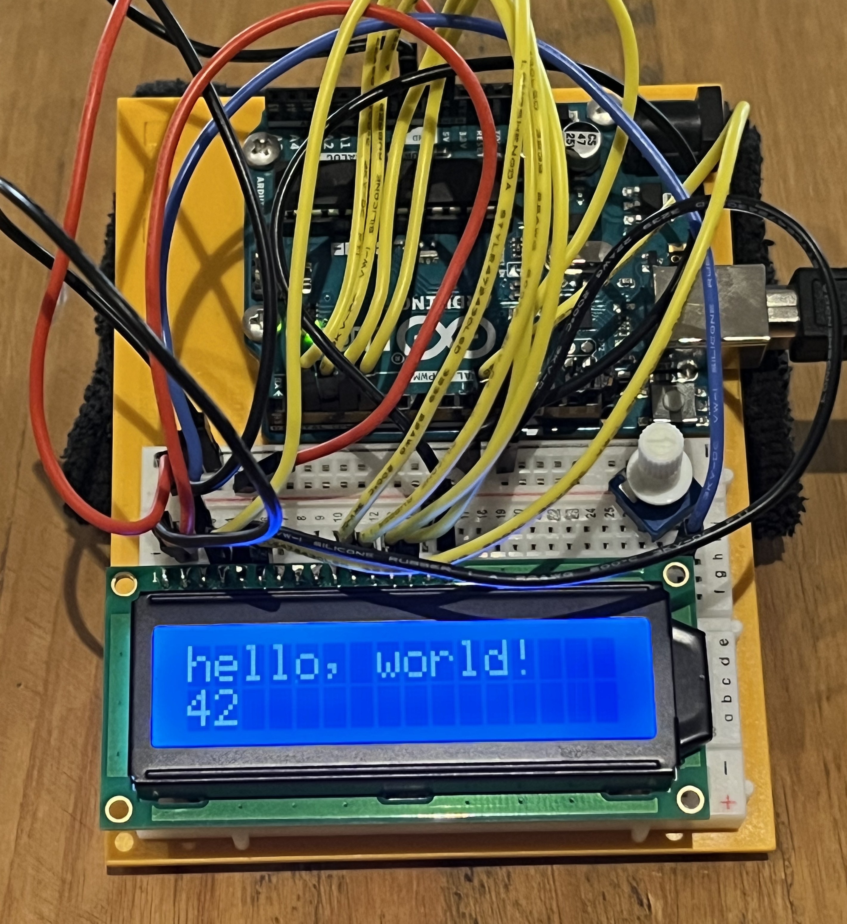
Nice clean design. I like to port some kind of BASIC onto my CPU projects to demonstrate they can do something, but now that everyone has access to cross assemblers and compilers it make more sense just to have a hex file downloader and let the user load anything they want. I shall be taking that approach in future, especially for CPUs for which I have no BASIC or other demo firmware.

  Are you sure? yes | no

Stephen Willcock wrote 03/25/2025 at 14:10 point

I like how it removes all the layers - you can follow the connections at a binary level, and hopefully that makes it a good learning tool for the fundamentals. That said, I do want to port a BASIC for the reason you give - especially when I add a keyboard and LCD. 

Oh and thanks again for the UM245R tip! 

  Are you sure? yes | no

Similar Projects

Does this project spark your interest?

Become a member to follow this project and never miss any updates