Design goals
I set myself to a list of very ambitious goals that I wish to achieve in this system::
- 16-bit data paths, primarily word addressable but with possible byte operations
- microcode control and CISC Instruction set
- Reduced amount of internal registers
- Memory protection by MMU and privileged operations
- Multiprocessing support
- C code compatible
- designed with the technology available in the mid/late 70s
- mostly on standard 74xx series, and if needed on S and LS
- no high-capacity SRAM or EPROM memories
- no microcontrollers
- reduced amount of programmable logic (PALs), PROM memories instead
- high performance of avg. 500 kIPS
- variety of IO interfaces and controllers
- modular construction
- variety of system configurations including dual processor one
System description
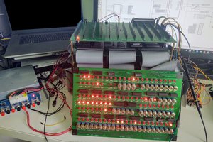
This AHCS is designed as a modular solution for various purposes. All system modules (despite slow IO controllers) are built on double-size Eurocard (220 x 233 mm) PCBs with two DIN41612 connectors, those modules are connected in a card cage using a custom wire wrap backplane. A basic system could be built with 5 cards: Two cards for CPU and one for MPC, IO bridge, and at least one memory card
CPU
The central processor module is based on unpopular Intel 3002 2-bit slice chips and is controlled by a 1k of 40-bit parallel microcode stored in fast RAM chips. The basic microcode cycle is 125ns but this could be extended by 1/3 of its time to 166ns in case of u-code conditional jump or if a longer data path is required. This basic u-cycle could be extended to around 1-2us in case of waiting for data from memory, after that request_timeout interrupt will be generated. CPU and MMU are integrated on two double-sized Eurocards, one for data paths and another for instruction decoding and microcode.
From the programmer's point of view, the CPU will have the following features:
- 16-bit data word, most operations use word addressing
- For word addressing 15-bit address, MSB is used for multi-indirect access instead
- For byte addressing 16-bit address, LSB selects high or lower byte
- Most of the instructions are single words but some less frequent are 2 words
- 8-addressing methods
- Two operation modes user and supervisor
- I/O, MMU, and interrupt control instructions are privileged
Cpu will have the following registers:
- Two universal accumulators A and B, could be combined into the 32-bit double accumulator D
- The lower byte of accumulator A is called accumulator C and it is used in byte operation
- Two universal indexing registers X and Y
- Two stack pointers one for the user and one for the supervisor and interrupts
- Program Counter and Frame Pointer - to simplify accessing local data on the stack
- Supervisor-only Flag register which controls the mode of the CPU
- There is only one ALU flag - the carry
MMU
Each CPU has its own MMU which converts its 15-bit virtual address into 19-23 physical addresses by paging
MCP
The Maintenance Control Processor is an 8-bit intel 8080-based microcomputer that has control over CPUs and access to the IO bus. It was mostly used during the system start. It contains a serial port for the maintenance console terminal from which commands are issued. When CPUs are halted the MCP provides monitor-like abilities:
- Accessing CPU registers including hidden ones
- Accessing main system memory
- Accessing IO devices
- Load CPU microcode
- Load main memory with system bootloader or test programs
- Single step and u-step the CPU
When the main CPU is running the MCP performs the following tasks:
- Provides programmable timers for OS for task-switching
- Provides real-time clock
- Buffers maintenance console which works as a system console
 Mikolaj
 Augusto Baffa
 Anders Dinsen
 Pawel Jablonski
 Dr PEKER