Sebastián Elgueta
Motivation
The capability to fabricate solid-state devices is a foundational technology which has deeply transformed our lives, and is expected to become even more relevant with the advent of data-heavy applications and energy harvesting/storage. However, the fabrication processes used require enormous capital expense, which has only grown with time. As a result, the tools required to create a functioning solid-state device are out of reach for many researchers in the field, and the increasing degree of consolidation in manufacturing capacity is effectively hindering innovation.
Main Idea
The main hypothesis behind the machine is that the fundamental (although not sufficient)requirement to generate solid state devices is to place the right material in the right place. While this is currently done through the Planar process in one of it's several variations, one could in principle just use a completely 'bottom up' approach where the required material (be it an insulator, conductor, extrinsic or doped semiconductor, among many others) is deposited in the required place.
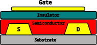
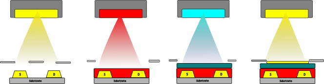
For example, let's consider a (cartoonish) Thin Film Transistor. A more serious description of it's fabrication can be found on resources such as 'The Art of Analog Layout' by Alan Hastings. In principle one just has to define the appropriate contacts, the active semiconductor region whose transport properties are modulated by the electric field, the gate insulator (usually a metal oxide) and the gate contact.
The approach used in this project is based on the combination of the following techniques:
Multi Material Pulsed Laser Deposition
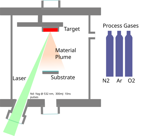
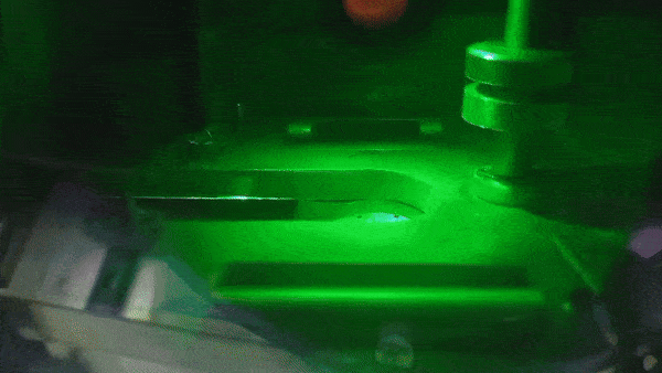
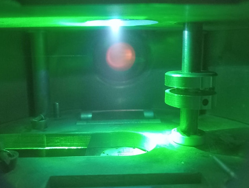
Pulsed Laser Deposition is a technique in which mass is transferred in a controlled atmosphere from a target to a substrate by means of irradiating the former with a high peak power pulse of light. The energy transferred induces out of equilibrium thermal processes in the target, resulting in the formation of a plasma 'plume' which has a stoichiometry closely matched to the target composition.

While it's not the technique of choice for industrial device fabrication (mainly due to film quality and complications associated with large area deposition, see this section), the ability to deposit a wide range of materials has made it the workhorse for many research regarding complex materials (oxides, nitrates, dichalcogenides, etc) and the applications of some interesting effects (ferroelectricity, superconductivity, …) that they show. An often overlooked characteristic of this technique is the ease of coupling of the energy over the target: one can control with exquisite precision the amount, rate, placement an timing of the energy transferred from the laser.
This simplicity allows a simple mechanical fixture to change the material being deposited:
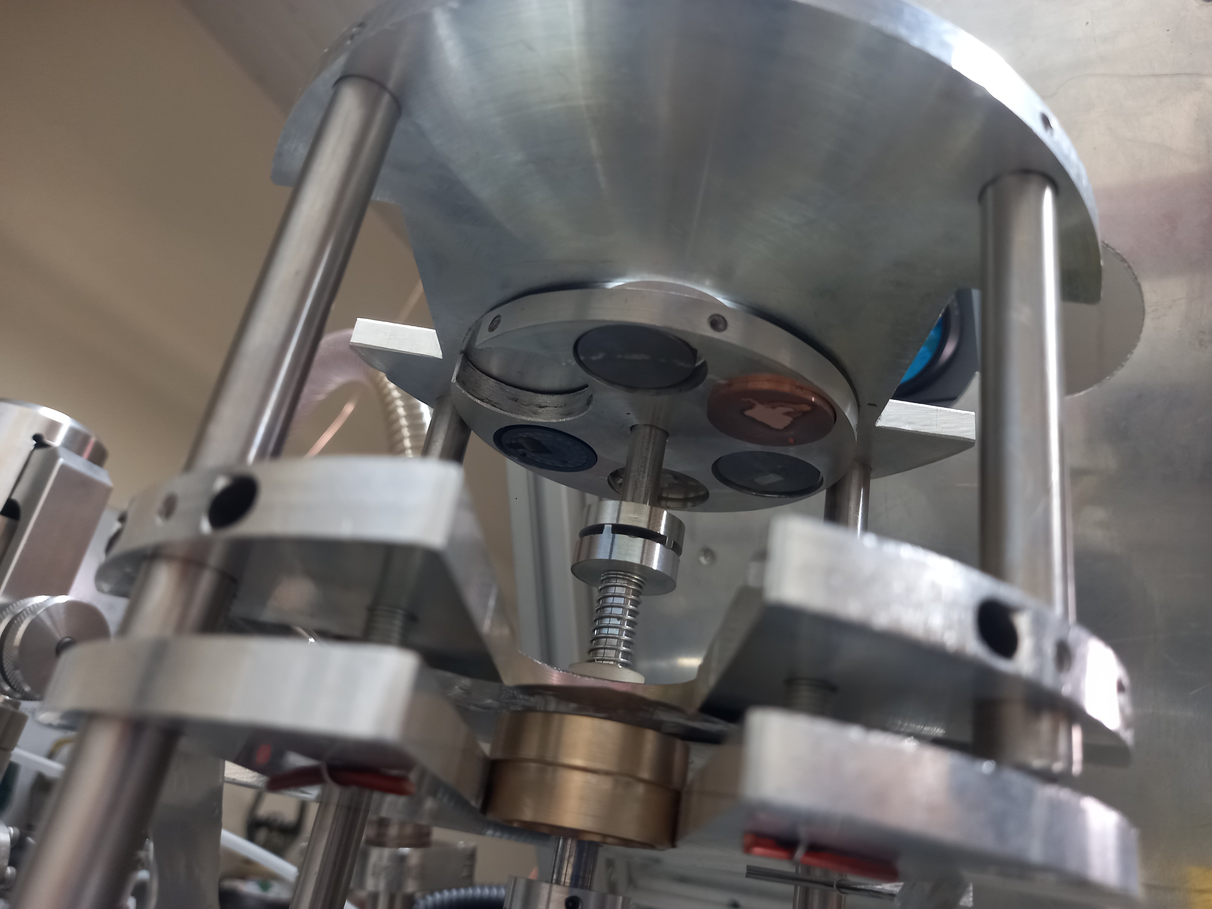
Then just a set of rotations allows oneself to greatly expand the kind of materials systems to be explored, from single materials to multilayers, alloys, (non)uniform doping, reactive deposition.

But this only allows the fabrication of thin films... a lithographic tool is needed in order to generate the patterns from which devices could be fabricated.
Shadow Mask Lithography
Also known as Stencil Lithography, it uses of a self-sustaining, usually solid mask with some defined apertures placed either in contact or some distance away from a substrate during a deposition process, which effectively allows the spatially selective transfer of material.
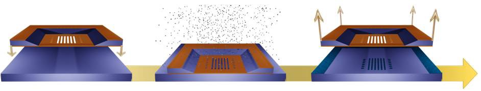
While this technique is seldom used in industry due to it’s practical resolution limitations, the spatial modulation of mass flow through an aperture is an inherently clean process which imposes very few limitations on the nature of the deposited species, as opposed to conventional resist based optical or e-beam lithography, where etching processes need to be carefully tailored to avoid undesired interactions, specially when there are underlying layers with very different physicochemical characteristics. It offers a series of benefits such as mask reusability, ease of manipulation, avoidance of resist contamination, loose constraints associated with substrate characteristics and the relative ease of implementation of dynamic lithography schemes, where the pattern moves with respect to the substrate allowing a grater deal of flexibility and some unprecedented capabilities regarding spatially tailored thickness and compositional variations.
In this case, the shadow mask are micromachined out of a 30 micron aluminum tape using a commercial fiber laser engraver (1064nm, 2W @ 30kHz).

While the repeatability quoted by the manufacturer is about 5 microns, thermal effects and the aspect ratio of the apertures limits actual feature size to structures in the 25 micron range.
While not spectacular, there is a major challenge when fabricating multilayered structures with different geometries:
Registration and Overlay
If we actually intend to make coherent structures, its critical that each feature and layer is aligned with the others, within errors that should be at least a third of the critical feature size.

For the current and target resolution, that implies submicron positioning accuracy, which is highly non trivial. While the first attempt in implementing the system used alignment marks with a feedback system, the added complexity made the project get a bit unmanageable.
As a simpler solution, the current system takes advantage of the lithographic tool (scanning galvo head) repeatability to ensure proper alignment. To do so, the idea is that if one fabricates the masks in place, both substrate and laser head could be static with respect to one another.
In situ Mask Fabrication
Mask fabrication is done through the aperture in the target carousel.
 After the 'bare' tape is moved in front of the substrate, the machining transfers the layer layout onto it.
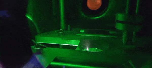
After the mask is ready (roughly 20min for my current designs, but it scales with the perimeter of the apertures), deposition begins:
For my current configuration (500 mJ in 6ns pulses, at 10 Hz, poor focusing) deposition rates are quite low, usually between (0.5-10 nm per minute, as it heavily depends on the material). Hopefully further iterations can provide better rates.
After the current layer deposition is over, the tape is displaced to repeat the process.