Close
0%
0%

Rapid Prototyping of Solid State Devices

A relatively inexpensive and flexible tool to generate heterostructures, devices and integrated systems

Public Chat
Similar projects worth following
A multimaterial physical vapor deposition system coupled with self-aligned, locally fabricated shadow masks. The system should in principle allow the deposition of a wide range of materials in a geometrically controlled way, effectively enabling the creation of heterostructures with quite a bit of functionality.
Hopefully one day might function as a tool for distributed manufacturing of ICs and other integrated systems.

Motivation

The capability to fabricate solid-state devices is a foundational technology which has deeply transformed our lives, and is expected to become even more relevant with the advent of data-heavy applications and energy harvesting/storage. However, the fabrication processes used require enormous capital expense, which has only grown with time. As a result, the tools required to create a functioning solid-state device are out of reach for many researchers in the field, and the increasing degree of consolidation in manufacturing capacity is effectively hindering innovation.

Main Idea

The main hypothesis behind the machine is that the fundamental (although not sufficient)requirement to generate solid state devices is to place the right material in the right place. While this is currently done through the Planar process  in one of it's several variations, one could in principle just use a completely 'bottom up' approach where the required material (be it an insulator, conductor,  extrinsic or doped semiconductor, among many others) is deposited in the required place. 

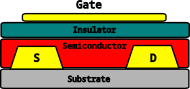
For example, let's consider a (cartoonish) Thin Film Transistor. A more serious description of it's fabrication can be found on resources such as 'The Art of Analog Layout' by Alan Hastings. In principle one just has to define the appropriate contacts, the active semiconductor region whose transport properties are modulated by the electric field, the gate insulator (usually a metal oxide)  and the gate contact.

The approach used in this project is based on the combination of the following techniques:

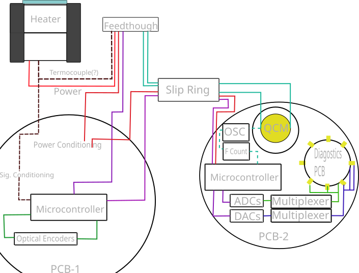
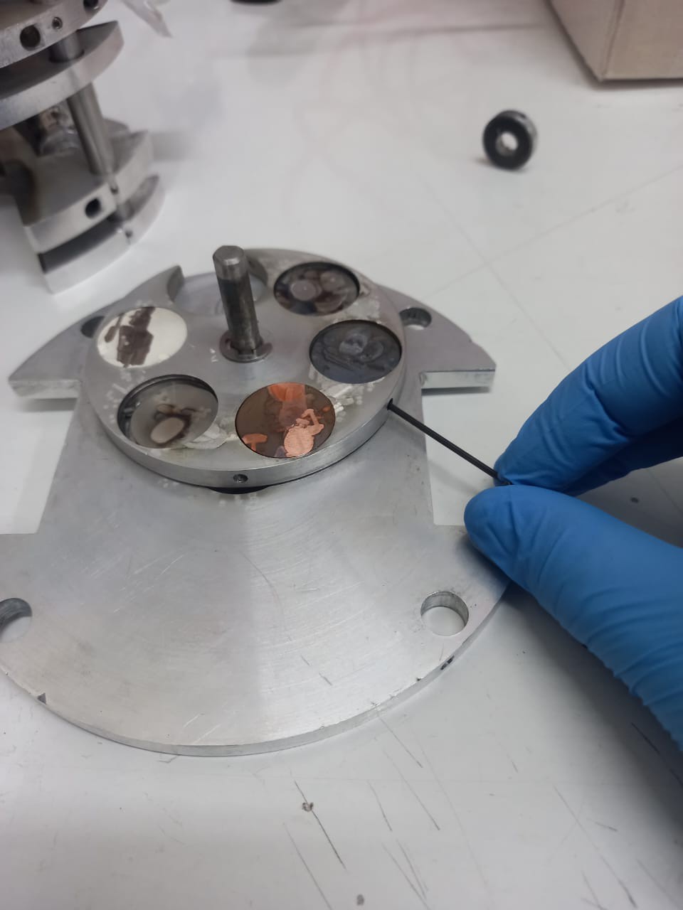
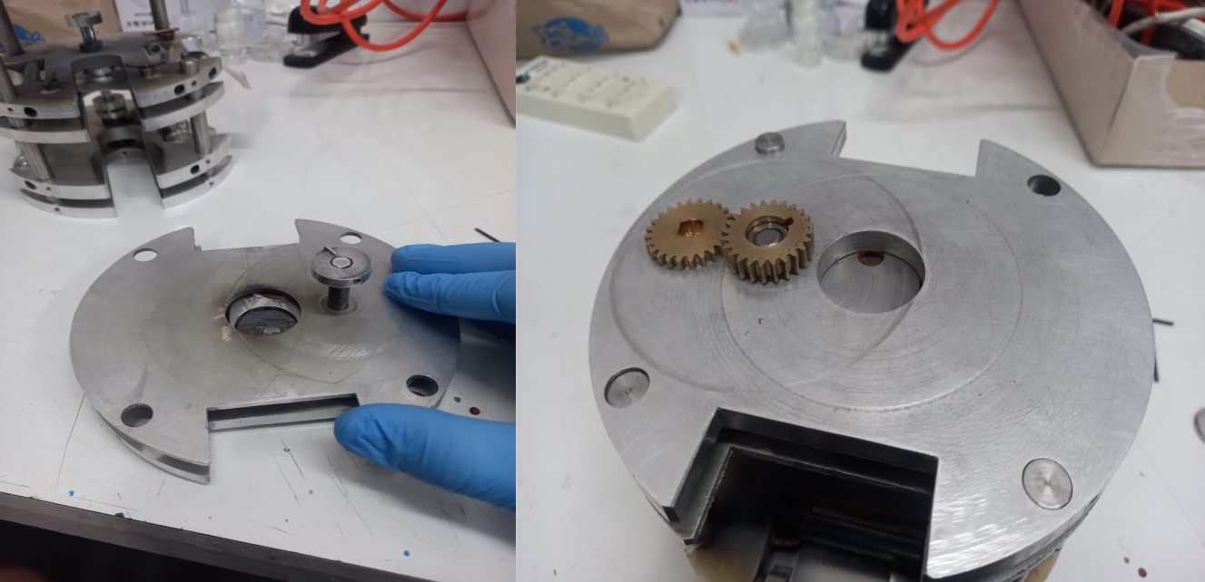
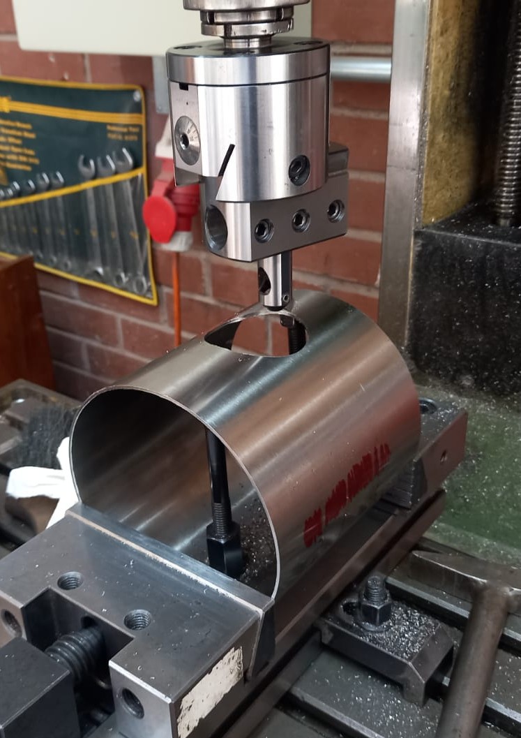
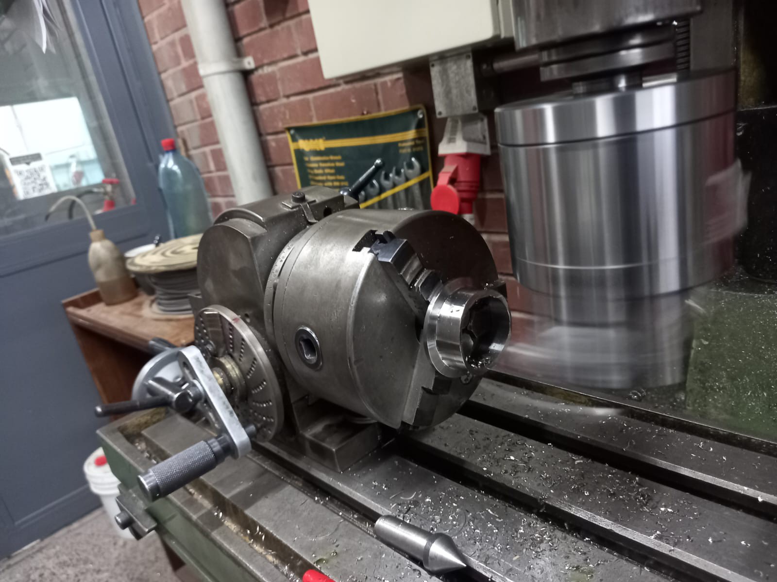
Multi Material Pulsed Laser Deposition

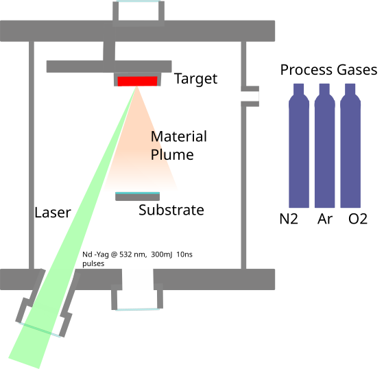
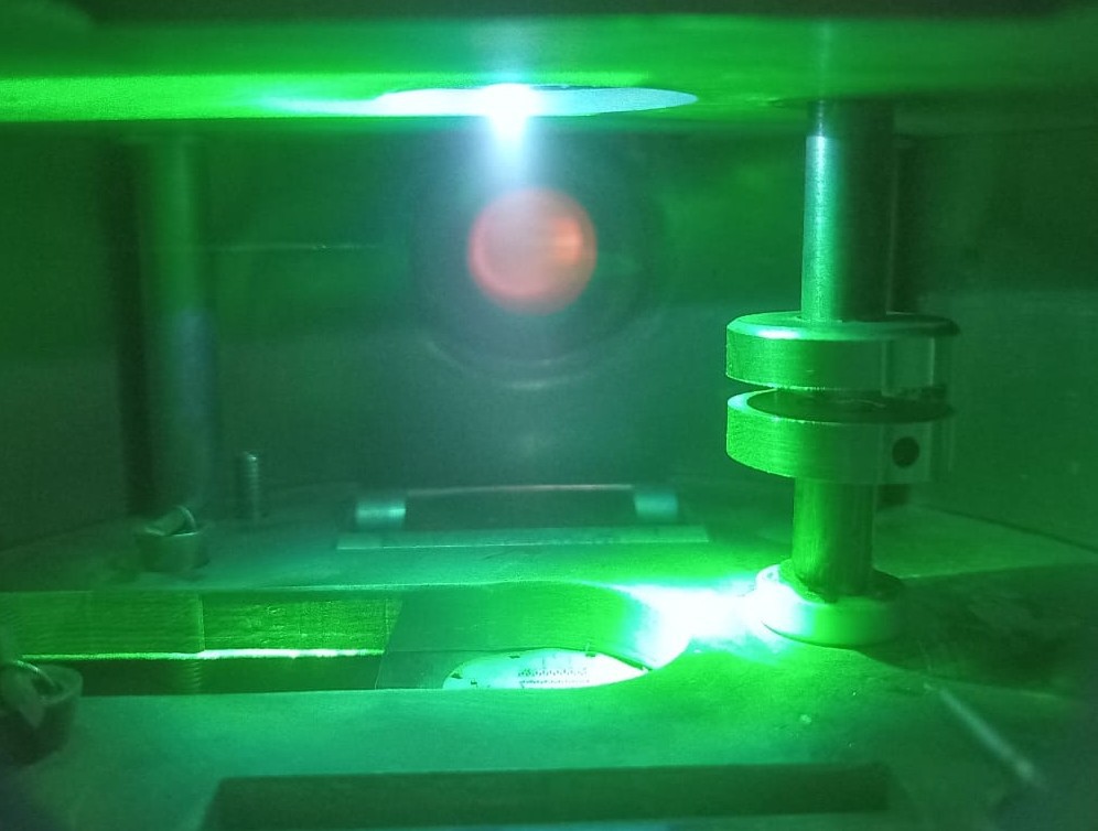
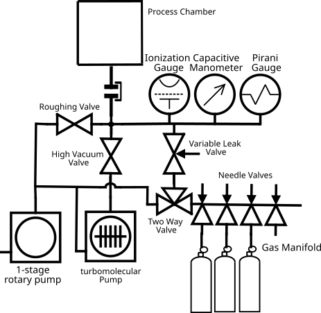
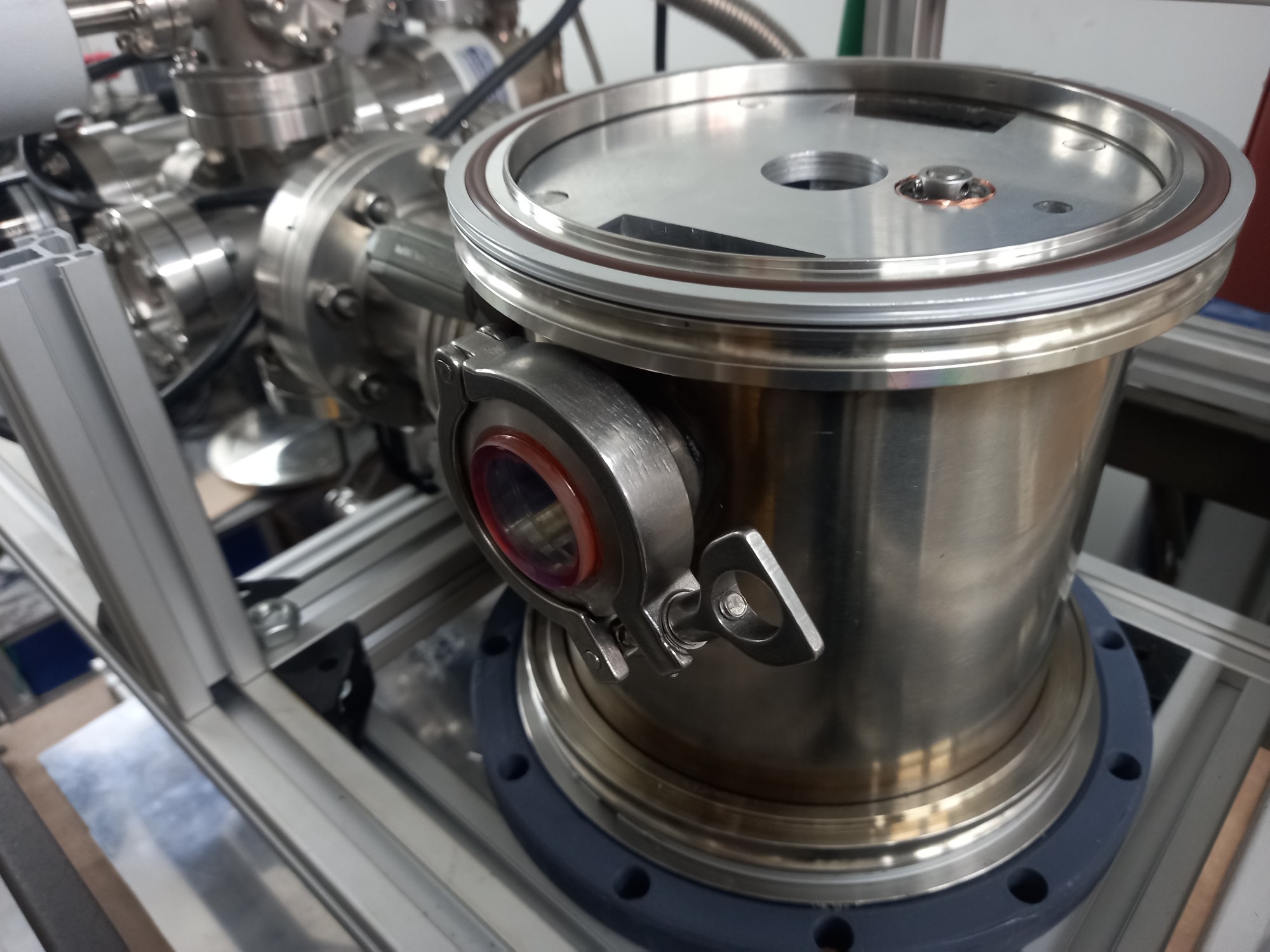
Pulsed Laser Deposition is a technique in which mass is transferred in a controlled atmosphere from a target to a substrate by means of irradiating the former with a high peak power pulse of light. The energy transferred induces out of equilibrium thermal processes in the target, resulting in the formation of a plasma 'plume' which has a stoichiometry closely matched to the target composition.

While it's not the technique of choice for industrial device fabrication (mainly due to film quality and complications associated with large area deposition, see this section), the ability to deposit a wide range of materials has made it the workhorse for many research regarding complex materials (oxides, nitrates, dichalcogenides, etc) and the applications of some interesting effects (ferroelectricity, superconductivity, …) that they show. An often overlooked characteristic of this technique is the ease of coupling of the energy over the target: one can control with exquisite precision the amount, rate, placement an timing of the energy transferred from the laser.

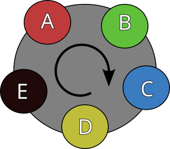
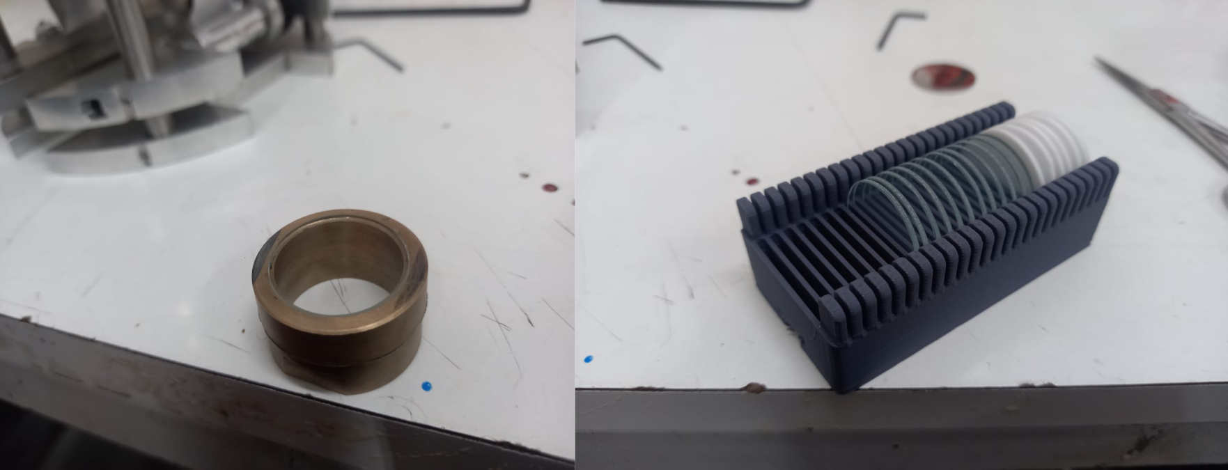
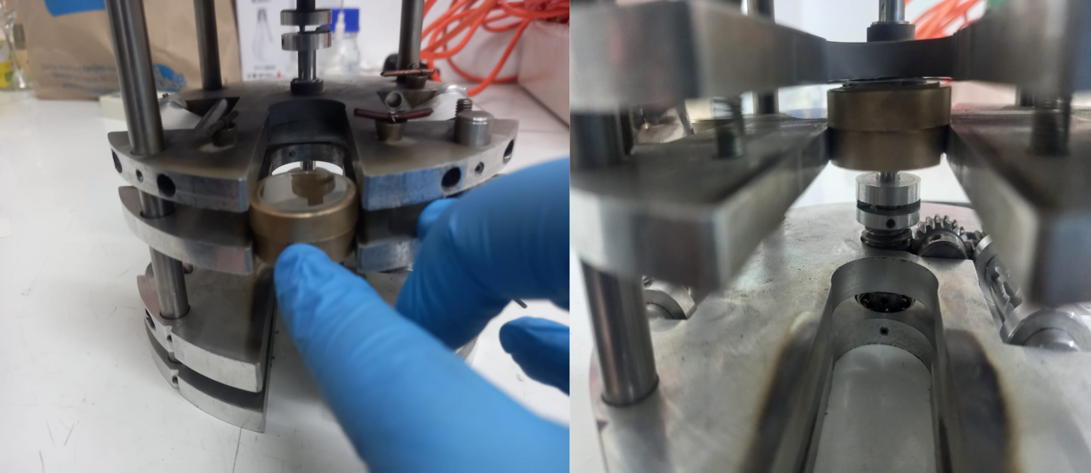
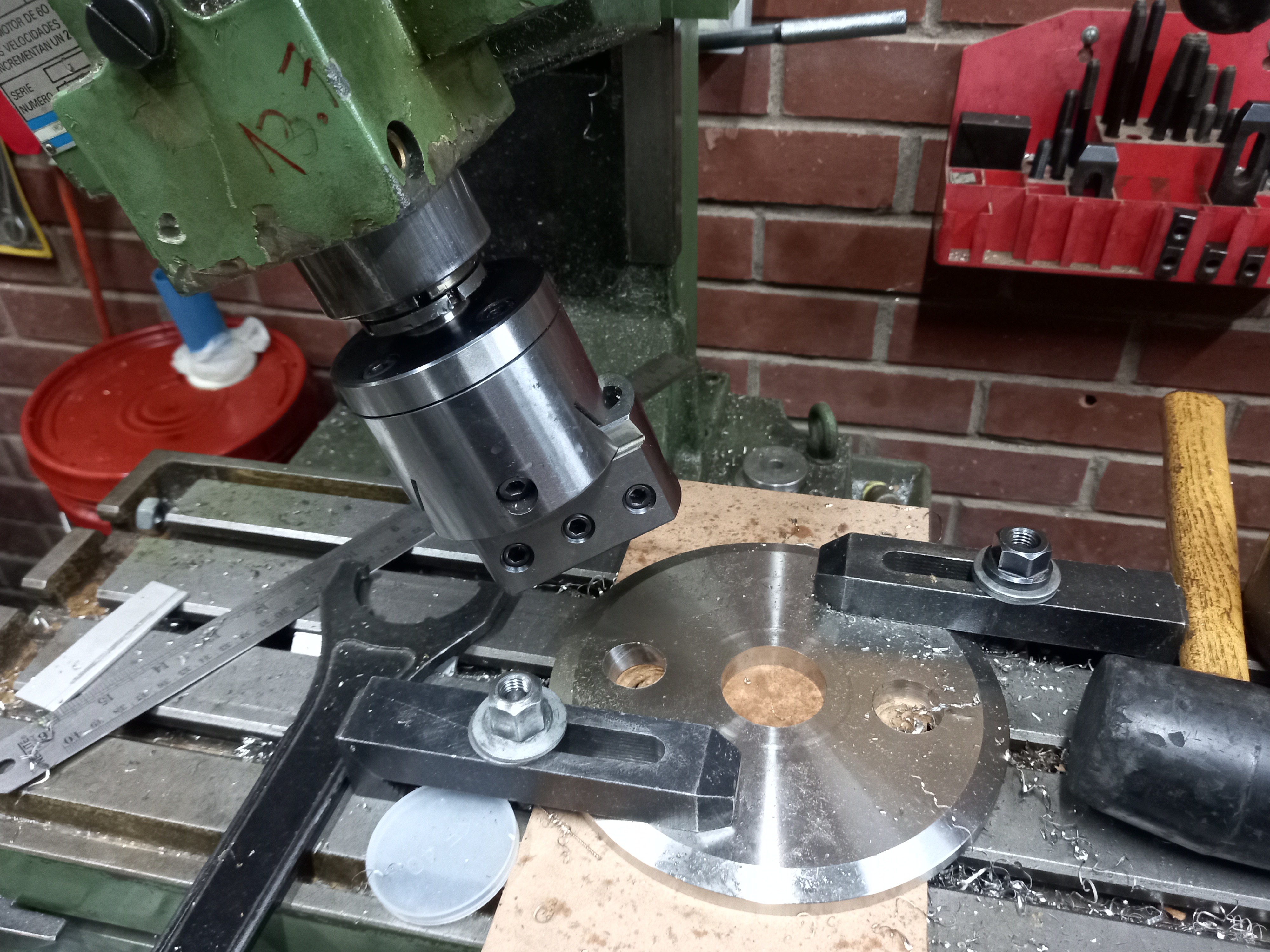
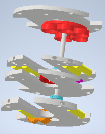
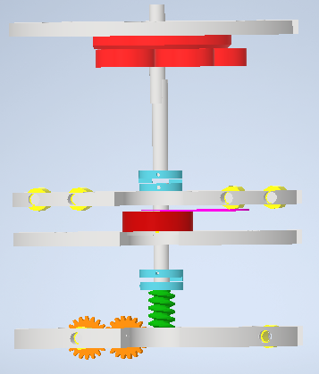
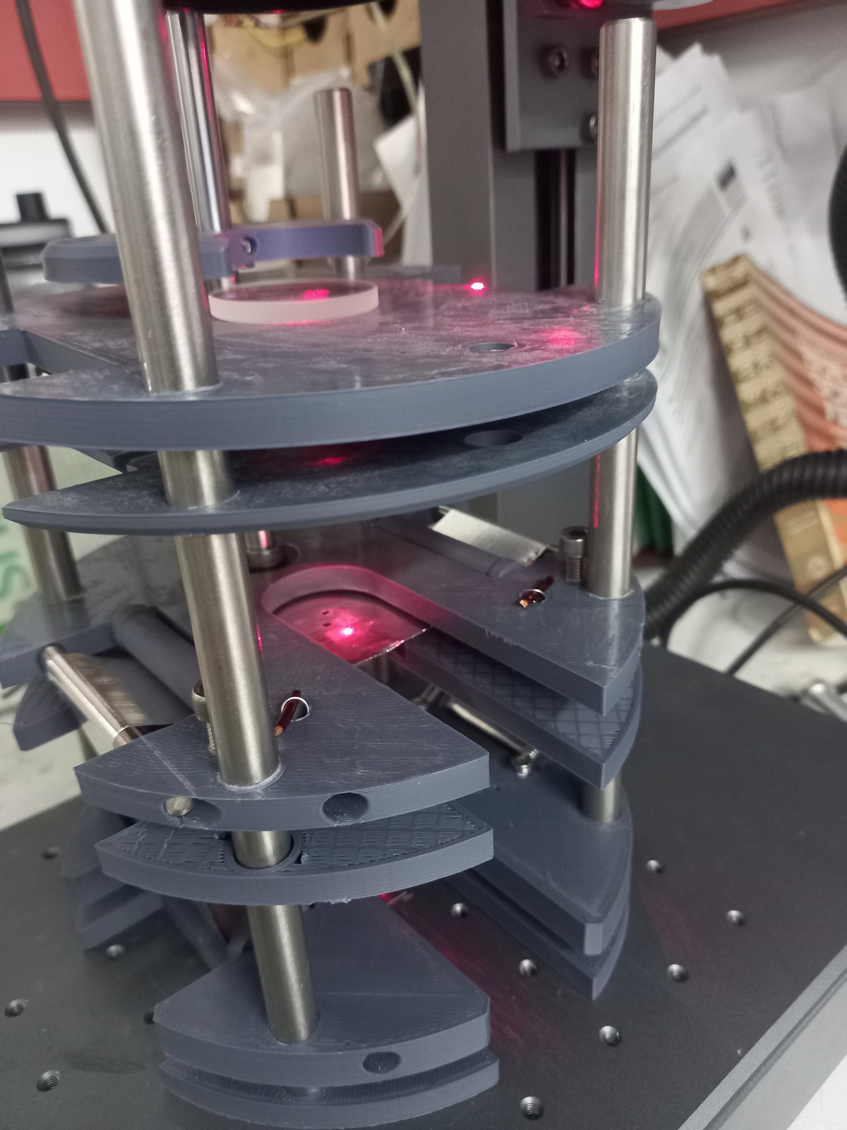
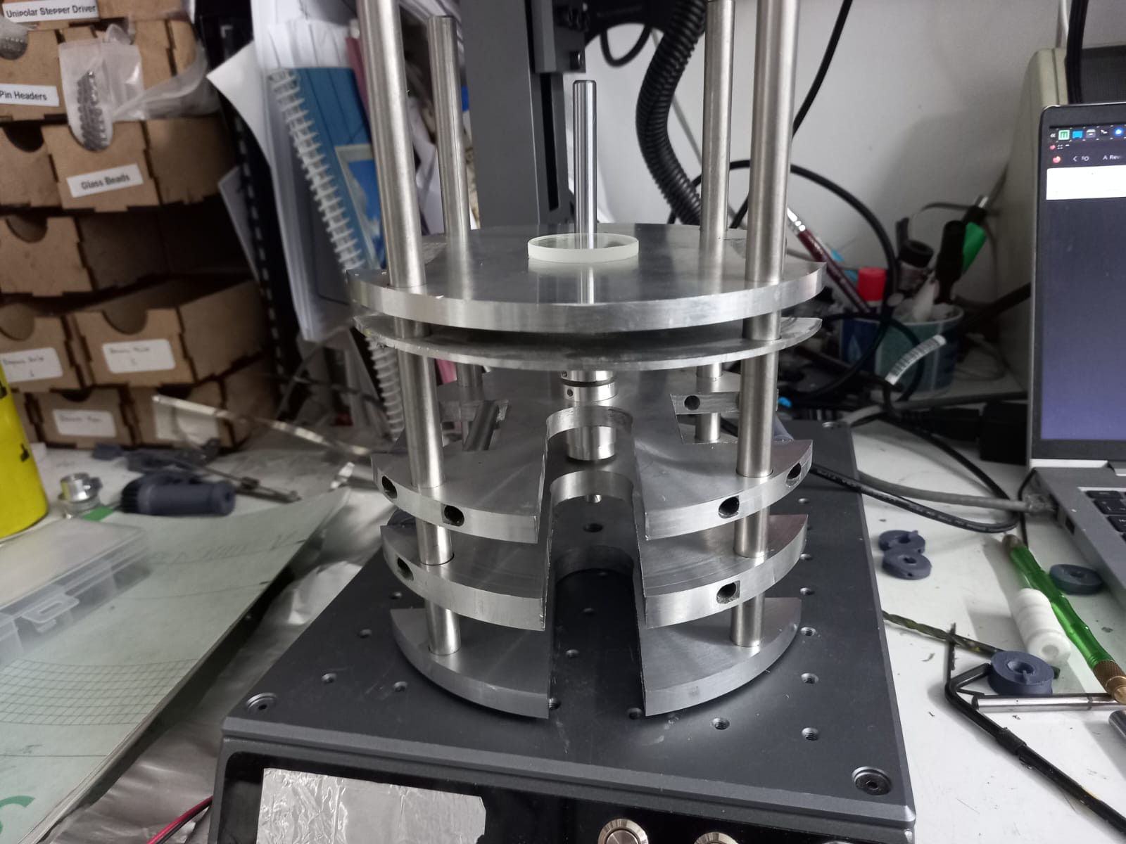
This simplicity allows a simple mechanical fixture to change the material being deposited:


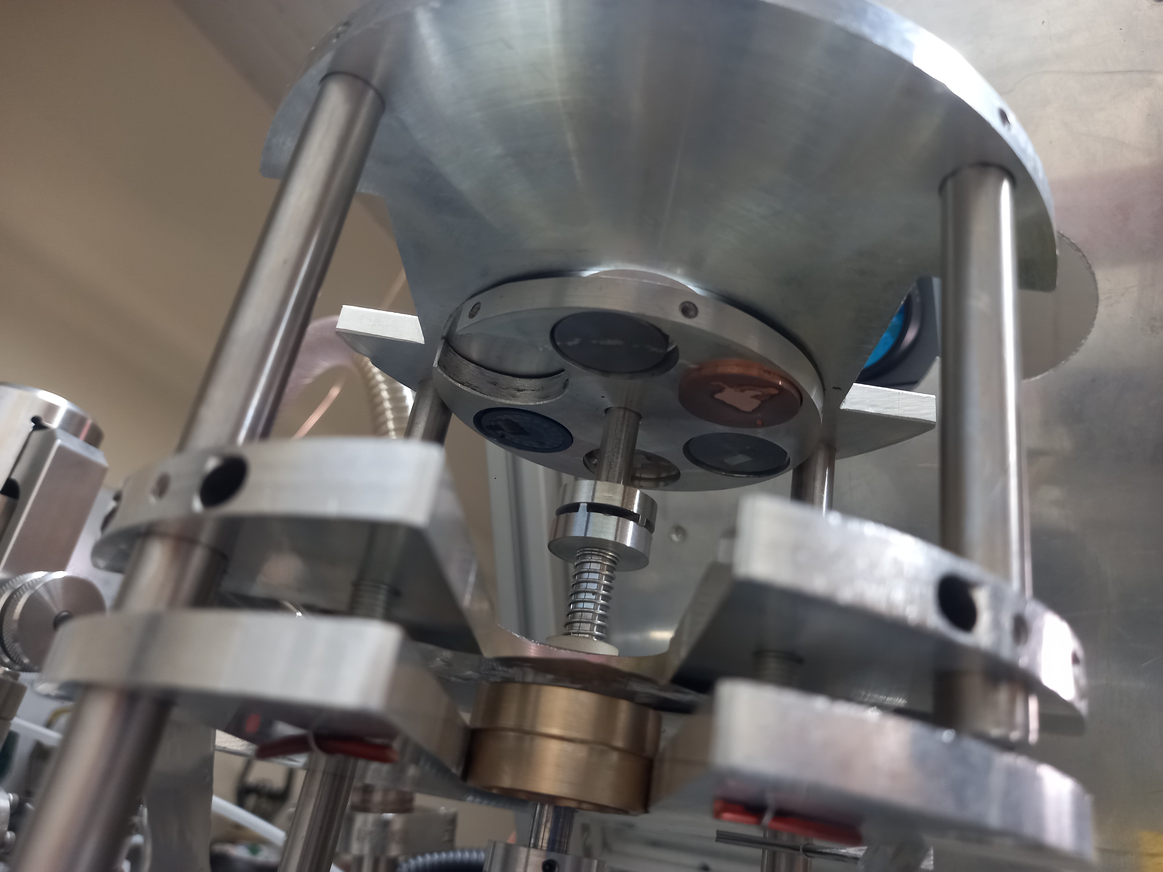
Then just a set of rotations allows oneself to greatly expand the kind of materials systems to be explored, from single materials to multilayers, alloys, (non)uniform doping, reactive deposition.

Deposition Posibilities
As each laser pulse usually ablates less than a monolayer of material, then depending on the length of each alternating cycle one may form alloys (if such phase is stable) or multilayers

But this only allows the fabrication of thin films... a lithographic tool is needed in order to generate the patterns from which devices could be fabricated.

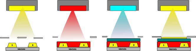
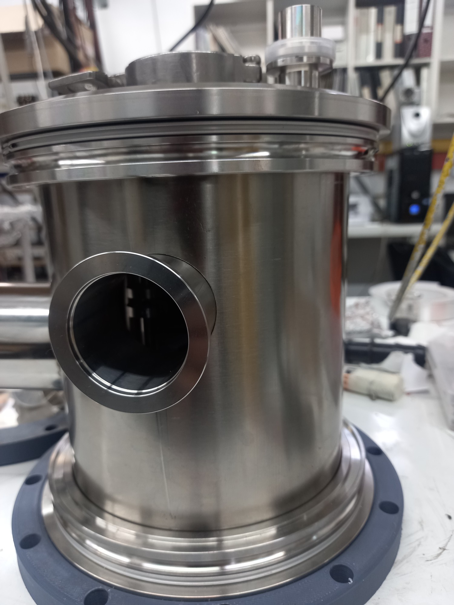
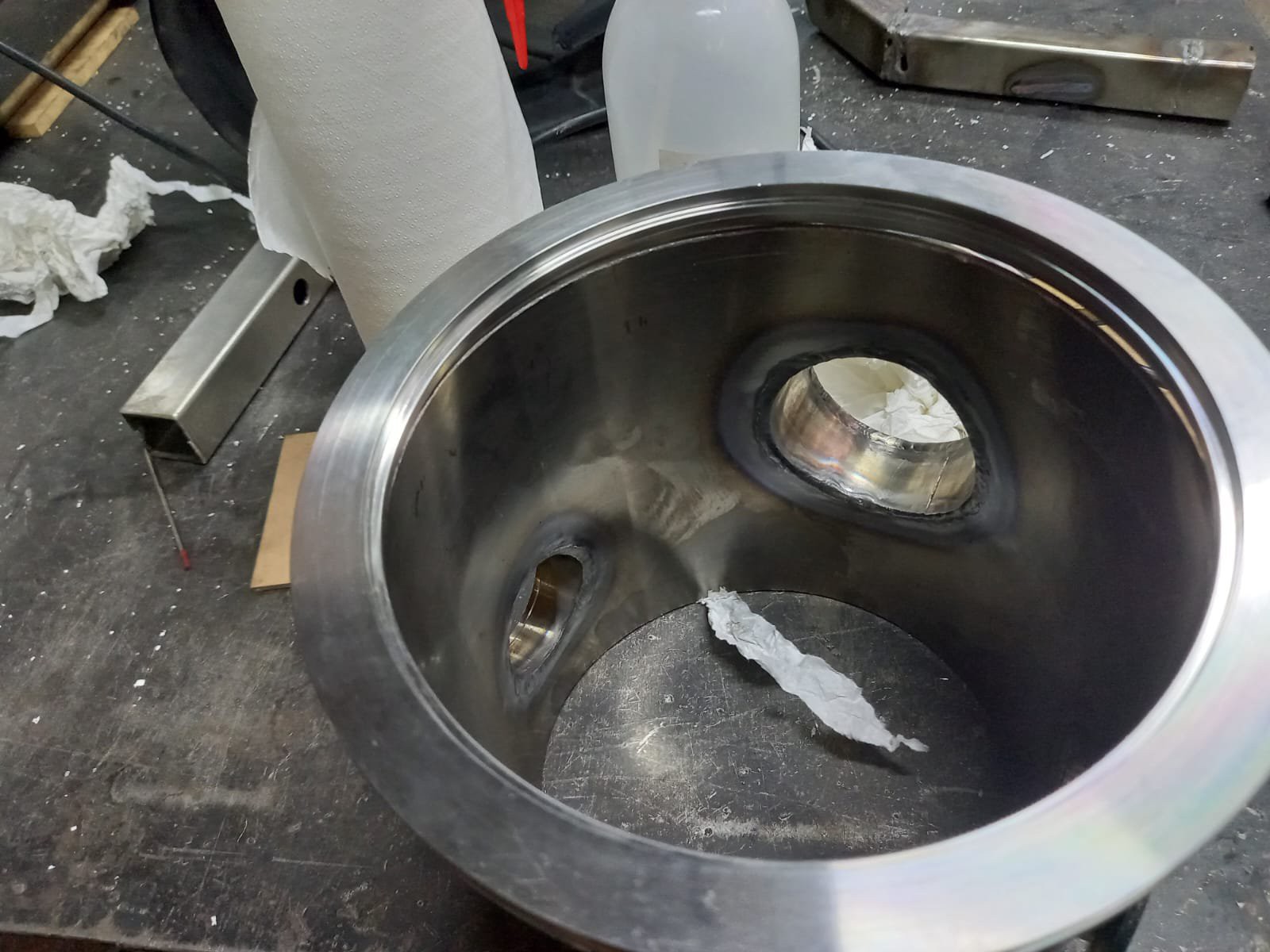
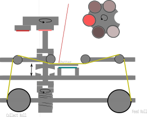
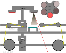
Shadow Mask Lithography

Also known as Stencil Lithography, it uses of a self-sustaining, usually solid mask with some defined apertures placed either in contact or some distance away from a substrate during a deposition process, which effectively allows the spatially selective transfer of material. 

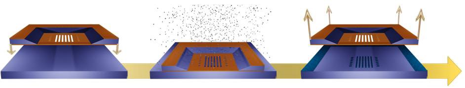
While this technique is seldom used in industry due to it’s practical resolution limitations, the spatial modulation of mass flow through an aperture is an inherently clean process which imposes very few limitations on the nature of the deposited species, as opposed to conventional...

Read more »

chamber_top.pdf

Adobe Portable Document Format - 170.96 kB - 02/04/2025 at 22:22

Preview

chamber_main.pdf

Adobe Portable Document Format - 177.70 kB - 02/04/2025 at 22:16

Preview

chamber_flanges.pdf

Adobe Portable Document Format - 177.51 kB - 02/04/2025 at 22:16

Preview

mask_stage.pdf

Adobe Portable Document Format - 458.05 kB - 02/04/2025 at 21:26

Preview

sample_stage.pdf

Adobe Portable Document Format - 457.69 kB - 02/04/2025 at 21:26

Preview

View all 7 files

  • In-Chamber Electronics

    Sebastián Elgueta02/18/2025 at 18:47 3 comments

    The Current Status

    At the moment, the system has no electronics inside the chamber, being  purely mechanic. This was an initial  design choice in order to simplify the initial design as a proof of concept. However, it's quite clear that the lack of any 'in chamber' diagnostics or feedback severely affects the whole system usability and reliability.

    As the proof of concepts was partially successful, it seems appropriate  to tackle the increased design complexity in  order to improve the rate of development.

    Goals and Constraints

    Overall, the intention of the proposed modifications are:

    Goals
    SolutionChallanges
    Enhance deposition
    quality
    A resistive substrate heater is incorporated
    Heat Dissipation, high current input, requires temperature feedback, possible damage to the tape
    Make the system more reliable and autonomous
    Positional feedback on the mechanical components status
    High pin count, relatively difficult mechanical placement of sensors, perhaps signal conditioning considerations
    Film Diagnostics
    In situ electrical measurements,
    Incorporation of a QCM sensor
    Required rotational electrical 'pass through', signal multiplexing is a must, connectors are no trivial

    Due to the evident space constraints inside the chamber, the rather small amount of available flanges and the cost of electrical feedthroughs,  I think it's quite clear that the way to proceed is to incorporate microcontroller(s) inside the chamber, which may reduce the pin count and allow signal transfer to the overall control system through serial interfaces.

    At least in my experience with vacuum hardware, this is a highly unorthodox solution, probably due to contamination and heat dissipation concerns. For the vacuum levels I'm working, the contamination doesn't seem as big a problem as the possibility that my electronics might get fried without precious air to dissipate the heat they generate. But let's trust metal-cored PCBs (and perhaps some exotic potting compounds) may help.

    The final constraint is the amount of pins available in the electrical feedthroughs. I  only have a couple of KF25 flanges available in the covers, and therefore I bought a couple  these feedthroughs:

    I have no idea about the current ratings, but I intend to use the thicker wires for the heater (which draws about 3A at 24V) while the 1.5 mm ones could be used to power the circuits inside.

     High Level Diagram


    While I still haven't fully committed with all the components and design choices (should I try to implement the QCM oscillator and frequency counter inside, or rather just use an external dedicated instrument, for example), the overall system is based on at least two PCBs: One coupled to the feedthrough cover, which hold the main microcontroller, which should take care of most of the IO workload (reading rotary encoders, communicating with the main controller, sending instructions to the other PCB) and a 'smart shutter', which replaces the existing one and holds the film diagnostics tools. Future logs shall dive deeper onto each of the systems components.

  • Current workflow and usage example: Part 2

    Sebastián Elgueta02/17/2025 at 14:06 0 comments

    Device Fabrication

    As outlined in a previous log, the design process mainly involves material selection, layout design and prepping the files for the laser cutter control software. Now it's time to see how the machine is used.

    Preparing the Mechanism

    Anyone who has worked with vacuum chambers knows that is usually not a breeze. While they are usually designed for modification by being quite modular, in the sense that the flanges allow changing the overall configuration  flexibly and access to the different components, it still isn't a process that is trivially easy nor practical.

    Therefore, ease of use was one of my primary design considerations, the idea being that changing material targets and substrates would be a quite frequent process while using the machine as a  material science research tool. In the standard configuration of PLD chambers, the target manipulator is usually fixed in a flange and therefore any changes are done inside the chamber, at least in my experience.

    For my design I opted for a 'capsule' arrangement, where most of the moving parts could be removed from the chamber, allowing easier 'servicing'. This design dates back to the first iteration

    The capsule itself is quite modular, consisting mainly on planar plates held together by rods, and arrangement which allowed to tune the different critical distances between the different components.


    Most of the components are fastened with M3 headless screws. So, first we fix the targets:

    And then proceed to add the protection plate (which is mainly to avoid the contamination of the targets with  aluminum from the tape machining process) and mount the top plate, along with the gears used to transmit the motion from the actuator to the main axis of the mechanism.


    The gears are required to provide clearance between the actuator and the laser head. Notice the notch on the left gear, which is used to quickly couple the actuator with the mechanism.

    Next one has to place the tape. Currently I'm using 35 micron aluminum foil, which is cut to a width of 35 mm and a length of about 1.5 meters. That in principle allows about 50 different mask, which in practice means that one has to change the tape after 10 deposition processes.

    The mask is fixed to the moving roller with aluminum tape (I know, not ideal), which is then properly placed by means of it's removable axle.

     Afterwards, I usually mount the substrate. I'm using  glass disks of about 25mm of diameter and 1mm thick, sold as watch covers.  They are cleaned with both IP alcohol, Acetone and DI water and mounted onto the substrate holder.

    The holder has a couple of notches which  mates to the 'substrate  plate', allowing the placement of the substrate under the mask tape without to much complications.


    Now it's time to discuss an important issue with the technique: The relation between repeatability and resolution.

    A conundrum: Mask-substrate distance and the shutter

    In case you recall, perhaps the main characteristic of the system is that the masks are machined in place, which in principle allows the whole system to 'inherit' the feature placement repeatability  from the lithography tool, namely the galvo laser engraver. Now the problem here is that laser micromachining is both a dirty ( as in producing particles that may contaminate the substrate) and an aggressive (in the sense that is quite easy to damage any surface placed closely to the mask ) process. The only solution I could came up that at least partially solves this two issues is to place a shutter between the mask and the substrate during the machining process. 


    The shutter is basically a thin plate made of sheet steel which is coupled to the main axis of the mechanism in such a way that it covers the substrate when the aperture of the carousel is in place. 

    While very effective to protect the substrate from laser damage and partially effective...

    Read more »

  • Current workflow and usage example: Part 1

    Sebastián Elgueta02/04/2025 at 20:04 0 comments

    Defining your structures

    While the system is still in a proof of concept stage, I think it's quite illustrative to see it functioning and the workflow that comes with it's usage.


    My (rather long term) plans involve making relatively complex integrated systems that might prove usable in real world applications, but there's plenty of work to be done to reach such goals. For example, each material used in the devices must be rather well known (though I would argue that 'optimizing' deposition parameter should be a later step), both in terms of the deposition parameters (deposition rate, adhesion to substrate/previous films, stoichiometry, overall quality) as well as it's functional properties (conductivity for conductors, doping density in semiconductors, dielectric constant and defect density in insulators, etc.)

    Therefore, I think that designing test structures to measure those material and process parameters is a good place to start.

     Workflow Overview

    1. Defining use case and structures
    2. Material Selection and Sourcing
    3. Layout Design
    4. Fabrication
    5. Testing

    Intended Devices

    The first step is to define the subset of materials to be used in the desired device(s). This is far from trivial, but hopefully a strong community is built around this processes which will help with streamlining such process.

    For this example, I'll try to implement a bottom contacts top gate thin film transistor based on Molybdenum contacts (for adhesion), Silicon as active semiconductor and Tantalum Oxide as gate dielectric, mostly due to availability. I don't know if the band matching between Mo ans Si can lead to a functioning device, but it's worth a try.

    The target carousel was designed to accept only cylindrical targets below 25.4 mm of diameter, and with a thickness not surpassing 6mm. Metallic foils can usually be accommodated also.

    PVD targets are relatively expensive, so I usually look for alternatives when possible. In this case both the Si and Mo targets are actually mirrors for laser cutting machines, which are substantially cheaper, although their actual composition is a mystery,

    Targets
    Si and Mo mirrors used as target, along with a proper PLD target (CuFeO2) for reference

    Making the Layout

    Currently I'm using Klayout through its Python API for mask design, and Lightburn for transfering the pattern. The tools are absolutely amazing, so much thanks for the respective developers, and specially to Matthias for open sourcing his tool.

    FIrst, I create the layers in the layout that later will map to a deposition step through one particular map.

    In this case  I used a layer for Silicon, a layer for Tantalum Oxide, and two layers for the metal (due to the kind of structures to be fabricated. More on this later), as well as two auxiliary layers: a visual reference  and  a layer to fabricate paths ('wires').

    Now one of the cool things about Klayout is it's ability define parametric cells. One may start from simple geometric primitives, and generate quite flexible structures. For example, the P_Cells.py  library holds some structures I found useful initially.

    Parametric Serpentine Resistor

    However, in these initial stages I was trying to diagnose some capabilities of the machine, and thus I was trying to implement different test structures to gather information such as achievable linewidth, step coverage, gap size, degree of alignment and registration, etc. I opted to generate structures where a geometric variable varied over a certain range, and for those cases I haven't been able to generate a proper PCell implementation, selecting straightforward coding instead:

    The file Struct_lib holds some functions to generate those kind of structures. As this was a demonstrative layout, I was interested in illustrating the process of making a TFT, so I kind of made an 'step by step' illustration;

    Now to connect the structures we have to add wires, which leads to an important issue with shadow masks: As they are self supported, not only they cannot replicate...

    Read more »

  • The Vacuum System

    Sebastián Elgueta02/04/2025 at 19:30 0 comments

    System Overview

    Performing the deposition in a controlled atmosphere is essential to generate films and structures with the appropriate characteristics. A decent vacuum ( ideally under 1e-6 torr ) and perhaps different low pressure reactive species (for examples O2 in the order of 1e-2 torr for oxides) must be alternated  in quick succession.

    Usually high vacuum pumps such as turbomolecular pumps operate within a narrow range of conditions, and turning them on and off is a time consuming process. Therefore, is important to design a vacuum system with a set of valves which allow fast variations among different atmospheres.

    This implementation took advantage of several components that I had available, which is far from ideal.

    Vacuum side view

    The Process Chamber

    While most components where taken 'off the shelf', the mechanism chamber had several dimensional requirements (specially regarding the target-substrate distance and the different lasers focal lengths) that could only be met with a custom chamber. As those are very expensive, I had to manufacture it myself.


    The cylindrical shape is quite standard due to it's ease of machining and good distribution of the pressure differential related efforts. I used a standard size for flanges, choosing ISO160 for their ease of use. I bought several Inner weld flanges from Aliexpress, as well as a 154mm OD x 2mm thick stainless steel pipe. Curiously I couldn't find any vendor from where I'm from, so I had to buy it abroad as well.

    The chamber was machined to length in a lathe, and then the aperture for the flanges where milled.

    The KF40 flanges, initially though as viewports and for plume diagnostics,  where bought from Aliexpress (they are fairly inexpensive) and then machined to provide the right fit to the main chamber:

    The same process was made for the ISO63 flange intended initially as a coupling to an existing turbomolecular pump.

    After making sure that the tolerances were acceptable, I proceeded to TIG weld the chamber together.

    While definitively not very pretty welds, after a few adjustments they seemed to hold a decent vacuum :).

    The process for the covers was quite similar: They also required custom apertures for the laser windows and manipulators. By mistake I bought KF160 instead of the proper ISO160 blind plates, but fortunately both standards are interchangeable.

    After the holes where bored, cheap KF(40/25/16) flanges were welded in place.

  • Making the 'Simple as Possible' Mechanism

    Sebastián Elgueta02/04/2025 at 15:40 0 comments

    Defining the process

    To being able to flexibly fabricate the intended structures, the following process was devised:

    One starts with a bare substrate, covered by the unmarked mask 'web' 
    and a shutter between them. The target carousel is placed in such a way that it lets laser light pass through it. Either under vacuum or an unreactive gas, the apertures are defined.

    When the apertures are cut, the shutter is removed and the proper atmosphere is set onto the chamber.  Then the proper deposition process is performed (either from a single target or a given combination).

    Once the deposition step is completed, the mask web is moved until only unmarked tape covers the substrate.  This sequence may be repeated until the mask is completely consumed.

    Evidently the shutter is required to protect the substrate from debris and laser ablation. It quite a compromise, as the distance between shadow mask and substrate heavily influences the achievable resolution.

    As a solution, the mechanism is designed in such a way that whenever the shutter moves into place, it pushes the substrate stage onto a lower position. When the substrate is uncovered, the substrate stage  reciprocates back, with it's position determined by a simplified kinematic coupling.

    Now such mechanism seems to have a fair bit of degrees of freedom: Target carousel, shutter, and mask roll movement is required. However, they move in a fairly well defined sequence, so in principle all movements could be partially coupled to one another in order to reduce the required actuation elements.

    A First Iteration

    The Prototype

    While 3D printed components are usually not vacuum compatible (at least not as is), they were a great tool to test the ideas involved, and gradually start implementing the final pieces. Here are a couple of pictures of the process:


    It was crucial to test the resistance of the tape after marking.

    Actual Mechanism Fabrication

    As the mechanism is mostly composed of planar 'plates' with different apertures, it's well suited for processing with laser cutters or waterjets. However, I wasn't very confident on my designs, so I rather chose to fabricate the whole assembly out of duraluminum stock.

    I started from a 6' cylinder , and turned it on the lathe to the appropriate (149 mm) diameter.

    After that, all the common perforations were made in a (relatively unsuccessful) attempt to keep al the plates and moving axis aligned. The common features between plates were machined as well:

    After that, each plate was cut from the main block (a royal PITA)

    And finished on the lathe:

    Or given some extra details in the mill:

    The process was repeated several times until the mechanism was completed:

    The remaining components (rollers, target carousel, couplings) were machined with standard techniques (and in those cases it actually made sense to do so).

    Evidently the manufacture could be simplified a lot using the proper tools to fabricate the plates, so I'm currently working on designing a mostly laser-cut version.

View all 5 project logs

Enjoy this project?

Share

Discussions

Meow wrote 02/20/2025 at 08:33 point

How are you going to dice the wafers and make wirebonds to a PCB or chip carrier?

  Are you sure? yes | no

Sebastián Elgueta wrote 02/22/2025 at 14:53 point

Hi! Not quite in that stage yet. I'm using an 3d printed jig holding an array of needle probes, which make contact with pads defined in the perimeter of the substrate.  Also the substrates currently used  as carrier for the devices are simple glass disks, so there's no 'economical' reason to dice them.

  Are you sure? yes | no

Dan Maloney wrote 02/20/2025 at 02:21 point

Fantastic stuff, can't wait to see more! This needs to get more attention, so I wrote it up for the blog. Should publish soon. Thanks for posting!

  Are you sure? yes | no

Sebastián Elgueta wrote 02/20/2025 at 13:36 point

Hi! Thanks for the writeup, it has been quite hard to properly communicate the ideas behind the project and you did a great job, much appreciated.

I'll definitively keep posting future developments, I'm quite committed to taking the current proof of concept onto an actually usable system :)

  Are you sure? yes | no

Similar Projects

Does this project spark your interest?

Become a member to follow this project and never miss any updates