 Sebastián Elgueta
Defining your structures
While the system is still in a proof of concept stage, I think it's quite illustrative to see it functioning and the workflow that comes with it's usage.
My (rather long term) plans involve making relatively complex integrated systems that might prove usable in real world applications, but there's plenty of work to be done to reach such goals. For example, each material used in the devices must be rather well known (though I would argue that 'optimizing' deposition parameter should be a later step), both in terms of the deposition parameters (deposition rate, adhesion to substrate/previous films, stoichiometry, overall quality) as well as it's functional properties (conductivity for conductors, doping density in semiconductors, dielectric constant and defect density in insulators, etc.)
Therefore, I think that designing test structures to measure those material and process parameters is a good place to start.
Workflow Overview
- Defining use case and structures
- Material Selection and Sourcing
- Layout Design
- Fabrication
- Testing
Intended Devices
The first step is to define the subset of materials to be used in the desired device(s). This is far from trivial, but hopefully a strong community is built around this processes which will help with streamlining such process.
For this example, I'll try to implement a bottom contacts top gate thin film transistor based on Molybdenum contacts (for adhesion), Silicon as active semiconductor and Tantalum Oxide as gate dielectric, mostly due to availability. I don't know if the band matching between Mo ans Si can lead to a functioning device, but it's worth a try.
The target carousel was designed to accept only cylindrical targets below 25.4 mm of diameter, and with a thickness not surpassing 6mm. Metallic foils can usually be accommodated also.

PVD targets are relatively expensive, so I usually look for alternatives when possible. In this case both the Si and Mo targets are actually mirrors for laser cutting machines, which are substantially cheaper, although their actual composition is a mystery,

Making the Layout
Currently I'm using Klayout through its Python API for mask design, and Lightburn for transfering the pattern. The tools are absolutely amazing, so much thanks for the respective developers, and specially to Matthias for open sourcing his tool.
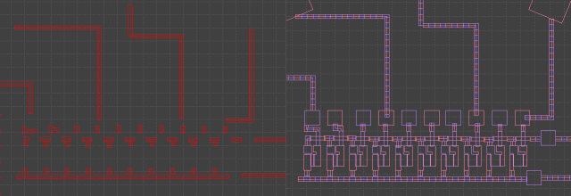
FIrst, I create the layers in the layout that later will map to a deposition step through one particular map.

In this case I used a layer for Silicon, a layer for Tantalum Oxide, and two layers for the metal (due to the kind of structures to be fabricated. More on this later), as well as two auxiliary layers: a visual reference and a layer to fabricate paths ('wires').
Now one of the cool things about Klayout is it's ability define parametric cells. One may start from simple geometric primitives, and generate quite flexible structures. For example, the P_Cells.py library holds some structures I found useful initially.

However, in these initial stages I was trying to diagnose some capabilities of the machine, and thus I was trying to implement different test structures to gather information such as achievable linewidth, step coverage, gap size, degree of alignment and registration, etc. I opted to generate structures where a geometric variable varied over a certain range, and for those cases I haven't been able to generate a proper PCell implementation, selecting straightforward coding instead:

The file Struct_lib holds some functions to generate those kind of structures. As this was a demonstrative layout, I was interested in illustrating the process of making a TFT, so I kind of made an 'step by step' illustration;

Now to connect the structures we have to add wires, which leads to an important issue with shadow masks: As they are self supported, not only they cannot replicate some geometries (think of a donut, for example) but also structures with long, unsupported features (consider, for example, the negative space of a pair of interdigitated electrodes) might deform under their own weight.
The solution is to make such structures in more than one deposition process, which is well suited for the current system. That's why some material layers have more tan one instance, to subdivide the structures into more than one.
To make the subdivision process easier, I use auxiliary layers (such as 'paths', in this case) to fabricate the original structures, and then the layout is fed to a 'Paths Post-processing' script which performs the required actions.
Now once the complete layout is ready, the GDS file is exported as an SVG using the script provided by Matthias onto LightBurn.
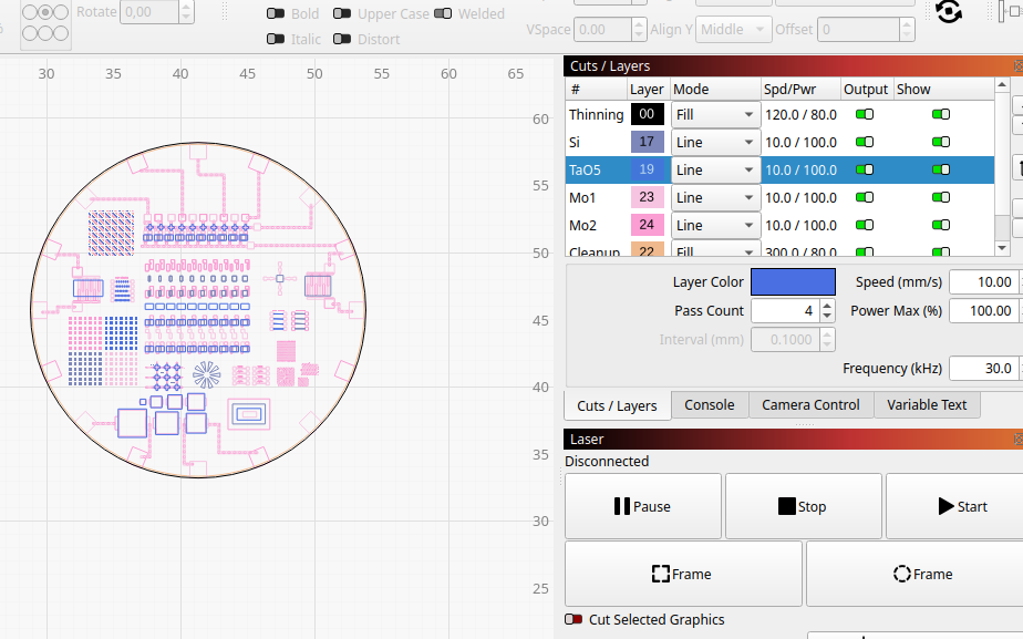
Here each (functional) layer in the layout is mapped to a given cut layer, where the laser parameters can be tuned according to the kind of structures. Currently the laser machining is mostly a photothermal process, and thus apertures with less perimeter then to require less passes. Each layer is thus selected (along with auxiliary processes such as mask thinnng and cleanup) and saved independently.
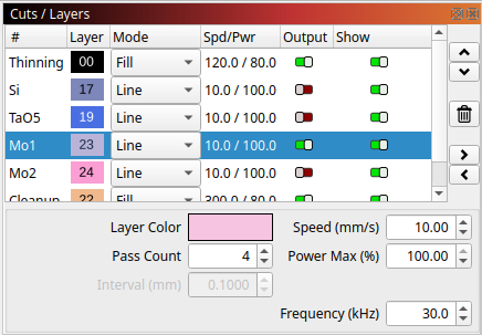
The filename is currently important for the automation process, I use the convention:
step[target1(time)target2(time)...]repetition.lbrn2
which is then intepreted by the machine control software. For example
0[F2B4]2.lbrn2
will be interpreted by the control software as the first deposition step, where a cycle of 2 minutes of deposition for target in position 'F' and 4 minutes of target in position 'B' is repeated twice,
The syntax is recursive, to allow the fabrication of the different possibilities for each layer.
So the folder fed to the control software looks something like:

Where each step of the process is assigned a given mask and a certain deposition parameters.
The control software and fabrication process will be outlined in the next log.
Discussions
Become a Hackaday.io Member
Create an account to leave a comment. Already have an account? Log In.