 Tony Francis
Last time, a plano-cylindrical corrector flattened the camera's focal bowl and pulled mean resolution to ~1.9 nm — about a 40% gain — by patching our conventional collimator + grating + camera build. That corrected the design we had. This log is a different architecture: In place of the collimator and the camera lenses and let one concave variable-line-spacing (VLS) grating do both jobs — disperse and focus 500–1000 nm straight onto the detector.
Up front: this one is modelled, not built yet — but modelled two independent ways that agree (analytic + ray trace), with all the code released. Posting it to get it constructive feedback before we commit.
The optical core
One concave grating, no separate mirrors:
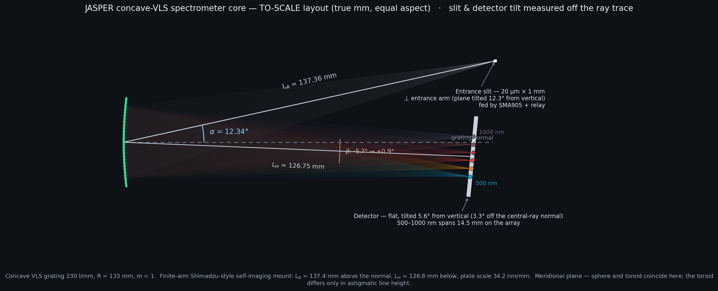
- Grating: 230 l/mm, incidence ~12°, arms ~137 / 127 mm, R = 133 mm.
- Plate scale: 34.2 nm/mm.
- Detector: 500–1000 nm disperses across ~15 mm — sits on any linear CCD ≥15 mm; a $10 TCD1304 (29 mm, 3648 × 8 µm) covers it with room to spare. The same grating reaches ~400–1100 nm (~20 mm) if you want the wider NIR range.
- Substrate — spherical vs toroidal: same resolution, but the toroid collapses the astigmatic line and boosts throughput ~25× (a throughput upgrade, not a resolution one).
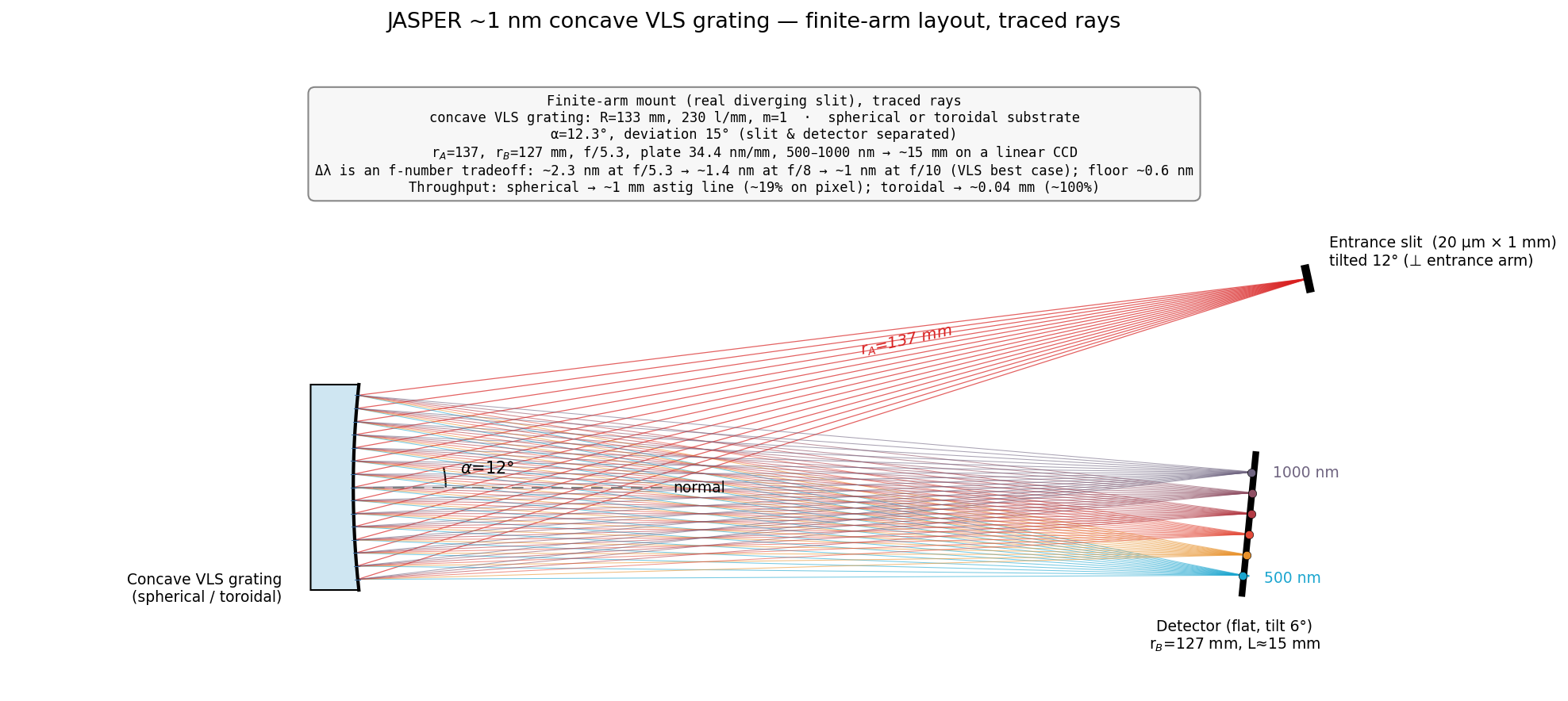
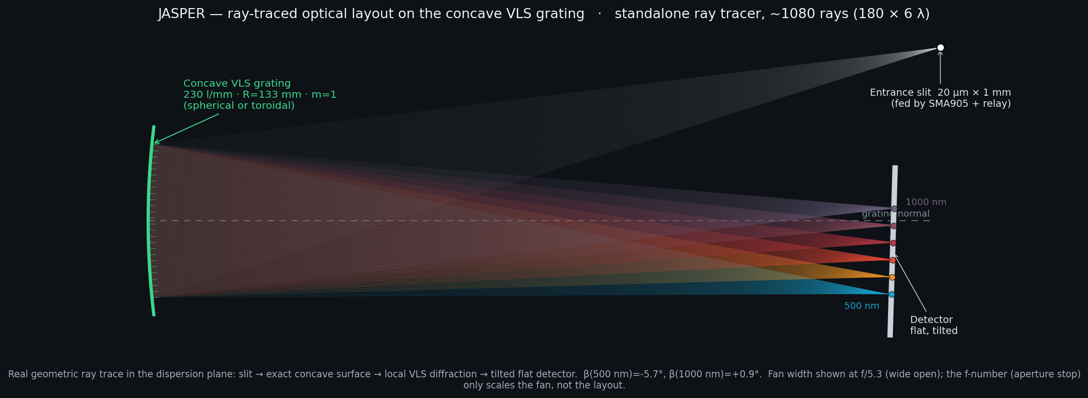
FIGURE: the optical core, real ray-traced (slit → concave surface → local VLS diffraction → tilted CCD), not a schematic
Resolution is an f-number tradeoff — not a single spec
The headline is a curve, not a number. Faster f = more light but more aberration; slower f + the VLS groove correction = sharper. Ray-traced across 500–1000 nm, three points along the path:
| working point | mean Δλ | 500 nm edge |
| f/5.3 spherical (wide open) | ~2.2 nm | ~2.7 nm |
| f/8 toroidal | ~1.4 nm | ~2.0 nm |
| f/10 toroidal + VLS correction (best case) | ~0.9 nm | ~1.0 nm |
| floor (slit + pixel + diffraction) | ~0.6 nm | — |
Takeaway: hitting ~1 nm across the band needs all three knobs together — stop down to ~f/10, use the toroid for throughput, and apply the VLS groove correction. None alone is enough. And the binding constraint is the 500 nm blue edge, which is aberration-limited (not slit-limited) — it's the last thing to come down.
On "best case": the ~0.9 nm assumes the fabricated groove correction matches the design. The uncorrected classical grooves are the guaranteed floor; the VLS number is the plausible target a real aberration-corrected grating is built to hit. We're posting all, for a fair comparison.
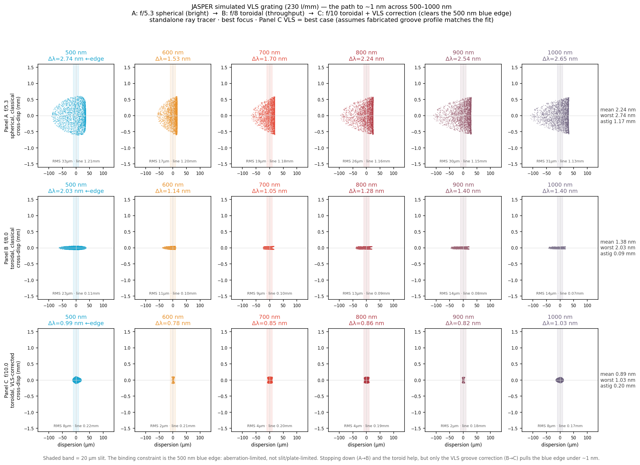
FIGURE: the f/5.3 → f/8 → f/10+VLS path to ~1 nm, real ray-traced spots
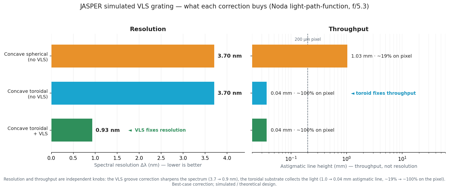
FIGURE: what each correction buys: the VLS grooves fix resolution (3.7 → 0.9 nm), the toroidal substrate fixes throughput (astigmatic line 1.0 → 0.04 mm). Two independent knobs, not alternatives.
Modeled two ways
We checked the design twice:
- Analytic — Noda–Namioka light-path-function theory (grating equation → dispersion; aberration coefficients → spot sizes from the mount geometry).
- Ray trace — our own standalone NumPy tracer, real rays through the exact surface with the local VLS equation.
They match exactly on dispersion and astigmatism. On resolution they diverge slightly — the ray trace captures higher-order aberration the 3rd-order analytic theory truncates — which is why the honest number is the f-number curve, not the analytic floor alone. (A tooling note: we started in Optiland but it couldn't hold dispersion and focus at once for this off-axis reflective mount; Beam4 can't model variable line spacing at all — so we wrote our own tracer, which also draws the ray-fan layouts. All code in the repo, retired experiments marked.)
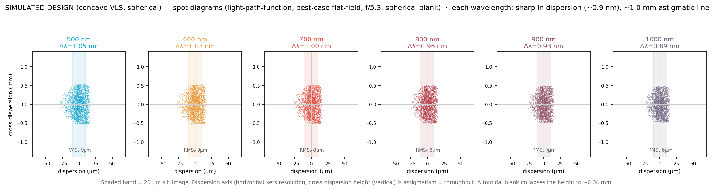
Code released
Full model + code (pure NumPy + Matplotlib):
https://github.com/CheckAG/JASPER_VIS_NIR_Optics_Design/tree/main/JASPER_1nm_VLS_simulated
Optical ray trace: (two formats, and pick which one you like)
What's next
Phase 2: the buildable side. Coupling a standard SMA fiber to the slit, and a real catalog grating (Shimadzu P0400-01, whose full mount is published) with the same f-number resolution story. Spoiler: the relay sets throughput, not resolution — the slit sets the line width.
Discussions
Become a Hackaday.io Member
Create an account to leave a comment. Already have an account? Log In.